
The European Union is undertaking a comprehensive overhaul of its Chips Act, which aims to increase the continent's share of global chip production; however, the legislation has largely failed to spur investment in new chip manufacturing facilities.
The Zhitong Finance app has learned that Europe's highest-valued company$ASML Holding (ASML.US)$An executive stated that the company currently does not sell any chip-manufacturing equipment in Europe, and as the United States, China, and India are making massive investments to develop their respective domestic semiconductor manufacturing and advanced packaging ecosystems, Europe faces a serious risk of falling behind in its supply chain.
At the time of this executive's remarks, products such as Meta's Muse and OpenAI's Astra have expanded the range of tasks they can perform autonomously, sparking a new wave of gains in the semiconductor sector of global stock markets. For ASML Holding, this means that demand for both advanced logic chips and advanced memory chips is expected to grow in tandem. Its position as the sole supplier of extreme ultraviolet lithography equipment—known as EUV—places it at the most critical upstream bottleneck in the AI computing power investment boom. Benefiting from the exceptionally robust expansion of AI semiconductor production capacity driven by the worldwide surge in AI infrastructure development, ASML's U.S.-listed ADR (ASML.US) has seen its share price soar by 60% so far this year. Meanwhile, two other major U.S.-based semiconductor equipment giants—$Lam Research (LRCX.US)$and$Applied Materials (AMAT.US)$The stock price has posted an even stronger gain, with year-to-date increases approaching 80% across the board.
 "We can't sell anything in Europe. That's because there's no investment there, and also because no chip factories are being built," Frank Hamskirk, ASML Holding's executive vice president for global public affairs, said at an event in Amsterdam late Monday.
Europe is home to globally leading semiconductor equipment companies, yet it lacks corresponding domestic investment in chip manufacturing. In the second quarter, Europe's net sales of systems to ASML Holding were zero; by comparison, the 1% figure for 2025 represents the combined net sales of systems across Europe, the Middle East, and Africa. These data highlight the gap between Europe's technological edge in equipment and its domestic investment in wafer fabs, and they also explain why executives are urging Europe to step up its efforts.
Wells Fargo & Co and another Wall Street financial giant, Citi, have recently revised upward their global forecasts for wafer fab equipment (WFE) spending, highlighting that, amid the booming global wave of AI computing infrastructure development and the broader "storage chip supercycle," semiconductor equipment manufacturers are also entering a period of extraordinary growth. They will be the primary beneficiaries of the rapid expansion in production capacity for AI chips—including AI GPUs, AI ASICs, and TPUs—as well as DRAM and NAND storage chips.
ASML Holding, Lam Research, and Applied Materials—semiconductor equipment giants—have all seen their stock prices surge in tandem with the broader semiconductor sector, outpacing the benchmark performance of semiconductor ETFs. At chip fabs, Applied Materials' presence is virtually ubiquitous. Unlike ASML, which remains firmly focused on lithography, Lam Research places greater emphasis on etching, cleaning, patterning, and critical thin-film processes, particularly high-aspect-ratio (HAR) etching and deposition—and related capabilities—essential for 3D NAND storage. Applied Materials' cutting-edge equipment plays a vital role in nearly every stage of chip manufacturing, with its product portfolio spanning atomic layer deposition (ALD), chemical vapor deposition (CVD), physical vapor deposition (PVD), rapid thermal processing (RTP), CMP, wafer etching, ion implantation, and other key steps in chip fabrication.
Global competition to expand semiconductor production is heating up, yet Europe's domestic efforts are facing tepid demand.
A senior executive at ASML Holding, Europe's highest-valued company, stated that the company currently does not sell any chip-manufacturing equipment in Europe; as the United States, China, and India make massive investments to develop their respective domestic semiconductor industries, Europe faces the risk of falling behind.
ASML Holding is a key pillar of the semiconductor supply chain, as it is the sole manufacturer of the precision lithography equipment essential for producing cutting-edge chips. Customers, including Taiwan Semiconductor and Samsung Electronics, use its equipment to pattern intricate transistor designs onto silicon wafers; these tools are also pivotal in driving the global artificial intelligence boom.
The European Union is undertaking a comprehensive revision of its Chips Act. Enacted in 2023, the legislation was designed to address semiconductor shortages during the COVID-19 pandemic and to increase Europe's share of global chip production. However, the law has largely failed to effectively stimulate investment in new chip manufacturing facilities. Last year, the EU's audit institution stated that the bloc is unlikely to meet its target of doubling its market share by 2030.
ASML Holding and the European Commission have been seeking ways to enhance the EU's technological competitiveness, strengthen its supply chains, and boost demand for chips. Meanwhile, other countries are injecting government funding and implementing additional incentives to promote domestic semiconductor production.
According to Heemskerk, the United States, China, and India are also actively seeking to persuade this chip equipment manufacturer to expand its local operations.
"We need to expand our production capacity, and this won't happen solely in the Netherlands," he said. "All parties are fiercely competing to persuade us to expand elsewhere. For ASML Holding, it's crucial that Europe takes proactive steps."
Heemskerk stated that China and India "rolled out the red carpet for us, saying, 'Come invest here too—build your factories right here.'" He added, "A quarter of our R&D is conducted in the United States, yet they ask, 'Can't we raise that to half?'"
In the second quarter, the individual European domestic market contributed zero to ASML Holding's system net sales, and the EMEA (Europe, Middle East, and Africa) figures have not yet been precisely aggregated. By contrast, in 2025, Europe, the Middle East, and Africa together accounted for 1% of its system net sales.
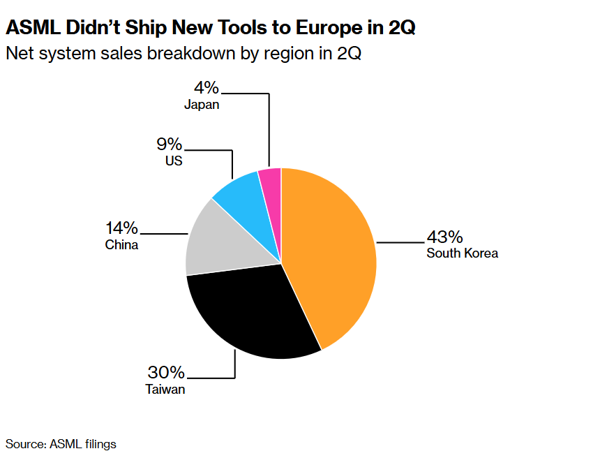
The chart above shows that ASML Holding did not deliver any new equipment to Europe in the second quarter—net system sales by region for the second quarter. Source: ASML's disclosed documents.
In the first half of the year, South Korea was ASML Holding's largest market for lithography equipment, particularly for its most advanced EUV lithography systems—both HBM and data-center‑related advanced DRAM capacity expansions require EUV tools—followed by the Chinese market. Notably, in May this year, ASML signed a cooperation agreement with Tata Electronics Private Limited aimed at boosting India's domestic chip‑manufacturing capabilities.
From the AI Agent Craze to Wafer Fab Capacity Expansion: The Dual Drivers of the Semiconductor Equipment Supercycle
From a global business perspective, ASML Holding's growth foundation is supported by the company's guidance and its capacity‑expansion plans. When the company announced its second‑quarter results in July, it raised its full‑year 2026 net sales guidance to €43–45 billion, explicitly stating that AI is driving demand for advanced logic and memory technologies, while customers are accelerating capacity expansion. Building on its current annual production capacity of approximately 65 low‑NA EUV tools and about 130 immersion DUV tools, the company plans to increase these figures by roughly 30% each in 2027 and is exploring further capacity expansion in 2028.
Therefore, the investment significance of the recent rapid advancements in AI agent technology lies in substantially and comprehensively bolstering the long-term sustainability of the existing trend toward expanded AI semiconductor production; the latest reports indicating that the United States, China, and India are actively vying for ASML's investment further underscores the global competition for semiconductor manufacturing capabilities.
From the perspective of its underlying architecture, an agent extends a single question‑answer interaction into a continuous workflow comprising "task understanding—planning—tool invocation—execution—verification." Pre‑filling entails processing the input context, decoding generates results in a streaming fashion, and key‑value caches scale with both context length and concurrency. Meanwhile, the browser, code execution, and external tools require coordinated use of CPU, memory, and storage resources.
Muse's dedicated virtual machines and Astra's multi‑step computational capabilities both exemplify this shift. Higher task success rates and lower execution costs, in turn, attract more workloads to AI systems. The resulting industry feedback loop is as follows: expanding application scope and scale drive growth in computing, storage, and interconnect capacity; this, in turn, spurs chipmakers to increase production and advance process technologies, gradually translating into heightened demand for hardware. These insights underpin the semiconductor‑industry‑chain demand trajectory rooted in AI inference system architectures.
Different equipment leaders cater to distinct manufacturing stages: ASML Holding primarily benefits from the expansion of wafer production capacity for advanced logic and advanced DRAM, as well as growing demand for critical lithography exposure; Lam Research, through its etching and deposition tools, plays a key role in fabricating 3D memory architectures, through-silicon vias, and advanced packaging interconnects; meanwhile, Applied Materials supports advanced transistors, HBM, and heterogeneous integration by providing technologies such as material deposition, planarization, metal interconnects, and wafer stress control. As chip architectures become increasingly three-dimensional, HBM stacking grows more complex, and packaging integration reaches higher levels, equipment investment is driven simultaneously by two factors: "the need to manufacture more wafers" and "the requirement for more sophisticated processes per wafer and package." The sustained, explosive growth of these two powerful demand drivers provides the strongest industrial rationale behind the global market's "semiconductor equipment supercycle."
Editor/Deng