
The AI computing power race is evolving from a mere battle over chips into a system‑level contest that encompasses interconnects, memory, and networking.
$Marvell Technology (MRVL.US)$Executives recently stated at the Six Five Summit 2026 that, as inference‑driven memory demand surges and data center scales push beyond physical limits, copper interconnects are approaching their performance ceiling, while optical interconnects and memory‑expansion technologies are emerging as the key enablers for the next phase of computing‑power expansion.
Will Chu, Executive Vice President of Marvell's Custom Cloud Solutions business, stated that the market has long focused on the XPU itself while overlooking the "adjacent layers" surrounding it—namely networking, memory, storage, and security. "Behind every XPU, there are three to four—or even more—customization opportunities," he said. "AI infrastructure is moving decisively toward full-scale customization."
 Dave Lazovsky, Executive Vice President of the Data Center Networking Business Group, noted that the rise of inference‑time computing has driven KV cache demand to grow roughly tenfold over the past nine months, outstripping the capacity of a single rack and necessitating scaling beyond it into larger interconnect domains.
This assessment carries direct investment implications for the market: memory manufacturers, optical interconnect providers, and custom silicon‑design firms will continue to benefit from this structural demand. Analysts forecast that cumulative capital expenditures for global data‑center infrastructure will reach US$4–5 trillion between 2025 and 2030.
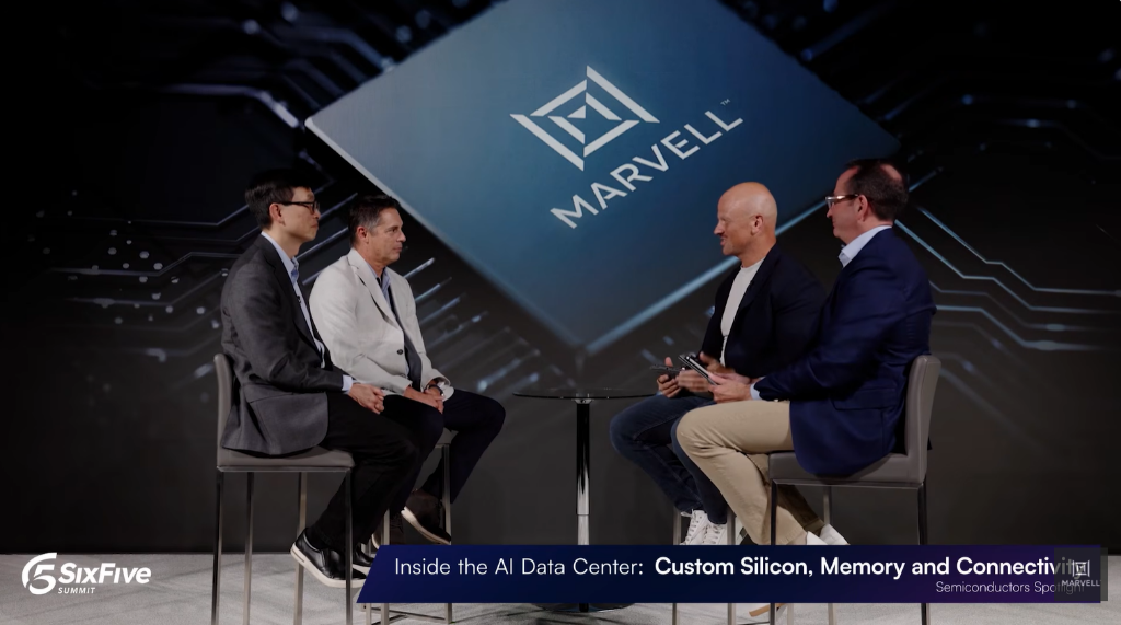
Copper interconnects are approaching their limits, and optical interconnects have reached a "must‑have" moment.
Dave Lazovsky characterizes the shift "from copper to optics" as a "mandatory requirement" for AI infrastructure, rather than an optional upgrade. The driving force lies in the evolutionary logic of the models themselves: the first-generation ultra-large-scale foundation models established a baseline demand for total memory capacity, while the rise of inference models, coupled with the explosive growth of KV caches, has rendered the HBM capacity within a single rack insufficient to support the operation of state-of-the-art models.
"You have no choice," he said. "You must scale the interconnect from 144 XPUs to the next‑generation Pod of roughly 576 XPUs, and continue scaling upward." The physical prerequisite for this expansion is switching from copper‑based interconnects to optical interconnects.
$Marvell Technology (MRVL.US)$Currently, the company is simultaneously advancing both on‑board optics (NPO) and co‑packaged optics (CPO) pathways, and has already deployed CPO solutions in switches compliant with Ethernet and UAL protocols. Will Chu added that Marvell can offer customers a seamless migration roadmap—from traditional copper solutions through NPO to CPO—and extend customization across the entire end-to-end stack, from compute units and I/O interfaces all the way to switch ports.
Dave Lazovsky underscored the differentiated value of Marvell's analog SerDes technology: compared with traditional 2.4T optical‑based SerDes links, scale‑up networks built on analog SerDes can cut power consumption by roughly a factor of four, and, once fully deployed, are expected to reduce overall data center energy use by more than 25%. Against the backdrop of severe power‑infrastructure constraints, this efficiency advantage is rapidly gaining strategic significance.
The Memory Wall: A Multi‑Layered Technological Portfolio to Tackle Exponential Demand
Will Chu characterized the memory bottleneck as the core engineering challenge confronting today's AI infrastructure, and broke down Marvell's response strategy into multiple layers, spanning from within the chip to beyond the rack.
Inside the chip, Marvell is deploying proprietary high‑density SRAM IP, which, through tight coupling with the compute units, boosts performance and enables larger models to reside on‑chip. He noted that conventional general‑purpose memory‑hierarchy designs can no longer keep pace with customer demands.
Externally, the pathways proceed as follows: integrating custom HBM to boost bandwidth and capacity; employing 3D stacking technology to place memory directly atop the logic chip; leveraging CXL or proprietary protocols for memory expansion, trading capacity for bandwidth; and, through Marvell's Photonic Fabric Memory device unveiled at FMS, delivering a 32 TB external memory pool within a dedicated rack space.
Dave Lazovsky further explained that this photonic‑fabric memory system seamlessly combines the capacity and cost advantages of DDR with the high bandwidth and multi‑pseudochannel parallelism of HBM, aiming to enable customers, for the first time, to scale memory capacity and bandwidth independently—fully decoupling them from compute resources.
Will Chu also noted that persistently high memory prices are compelling hyperscale cloud providers to reassess their overall infrastructure architectures. Marvell's CXL products have already garnered significant demand, partly from customers seeking to integrate legacy memory into new servers and achieve twice the effective capacity through memory compression. Meanwhile, flash‑tiered memory‑hierarchy solutions are gaining traction as a lower‑cost option for expanding storage capacity.
Scale‑out Networking: Customization Has Become the Standard for Hyperscale Providers
Dave Lazovsky pointed out that currently, about four companies account for more than 75% of the total addressable market for data center infrastructure. This highly concentrated market structure results in…$Marvell Technology (MRVL.US)$It is able to implement a business model that stands in stark contrast to the service‑centric, fragmented customer base—deeply integrating itself into customers' development teams and collaborating several years in advance to co‑architect the requirements for next‑generation switches.
He outlined three primary pathways for scaling up networks: some vendors favor Ethernet‑based solutions; another approach employs the UAL protocol, a high‑performance, memory‑semantic load–store network akin to NVLink, which Dave Lazovsky argues is inherently more efficient than Ethernet's packet‑based transmission; and yet another vendor is deploying a fully proprietary, custom‑designed topology.
Will Chu added that the tight coupling between XPU and the scale‑out network inevitably necessitates deep customization of both the protocol stack and optimization strategies, ultimately resulting in a custom silicon implementation. "Not every company can deliver an end-to-end solution," he said. "But we not only can—we also serve as an extension of our customers' development teams, directly participating in the design of their most critical infrastructure."
Dave Lazovsky also stated that Marvell's long-standing relationships of trust with leading hyperscale customers and GPU manufacturers are among the company's most valuable assets. "These relationships take years to build, and we already have that trust in place."
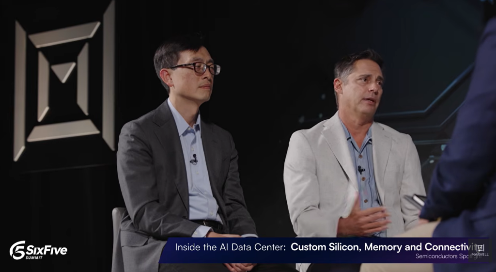
The full transcript of the interview is as follows:
Patrick Moorhead|00:17
Welcome to the Six Five Summit 2026. This year's theme is "Unleashing the Potential of AI." Joining me as co-host is Daniel Newman. How have you been, my friend?
Daniel Newman|00:38
Very good. This year's changes are truly remarkable: while computing power remains critically important, connectivity technologies have taken center stage, sparking extensive discussions.
We've been cycling from one bottleneck to the next. As you pointed out, connectivity has taken center stage, but this year we've practically run through every major constraint: first it was compute power, then CPUs eclipsed GPUs in importance, and soon after, memory became the linchpin. Later, the focus shifted not just to connectivity but further toward optical interconnects. And if you like, we could even talk about energy. Pat, with one hot topic following another, this year has truly been a rollercoaster.
Patrick Moorhead|01:02
We're now at Marvell's headquarters, and next we'll be discussing custom chips, memory, and interconnect technologies. Let me introduce Will and Dave—great to see both of you.
Dave Lazovsky|01:14
Thank you very much for inviting us.
Patrick Moorhead|01:16
I'm really looking forward to this exchange. I've seen you speak on stage and have attended your analyst days and product briefings. It's wonderful to have you here at Six Five today.
Daniel Newman|01:26
It's great to have both of you here, and congratulations! I understand you recently completed an acquisition, and from what I hear, it's been going very smoothly. Of course, there's still plenty of work ahead.
Pat, you mentioned connectivity technologies. What's interesting about Marvell is that it's involved in virtually every layer: chips, memory, and connectivity—plus scale-up, scale-out, and scale-across. It has a presence across all these domains, doing whatever needs to be done.
Daniel Newman|01:49
Do you think everyone knows the movie "Mr. Mom"? I think they do. Let's wait and see.
Will, let me ask you first. The business you're leading is one of the fastest-growing in the semiconductor sector. I recall Jensen Huang once called you the next company to reach a market capitalization of one trillion dollars. That certainly brings some pressure, but you're indeed already moving in that direction.
Daniel Newman|02:12
It's fair to say that, over the past few years, Marvell has largely risen into the spotlight thanks to its custom‑chip business. However, your portfolio also encompasses memory‑expansion architectures, vertical‑scaling interconnect networks, and cross‑domain connectivity—covering a remarkably broad range of domains.
I'd like to hear your perspective from a holistic business standpoint. The market is closely watching XPU and custom chips—what aspects of this attention are well‑founded, and what key factors are being overlooked? As mentioned earlier, the forces driving this wave of AI enthusiasm are multifaceted; it's not solely about XPU itself.
Will Chu|02:52
That's a good question, Daniel.
Daniel Newman|02:54
It took quite a while of setting the stage before I finally managed to get the question out.
Will Chu|02:55
Thank you as well for joining us at Marvell. The market indeed views the XPU as a key, custom‑designed component of AI infrastructure. Accordingly, we've devoted considerable time to introducing what we call "XPU Attach"—the suite of complementary components that surround the XPU.
Overall, we observe that every aspect of AI infrastructure is moving toward customization. While the XPU itself must, of course, be tailored to specific workloads, so too are all the surrounding components—networking, memory, storage, and even security. These constitute the key categories, and we are involved in all the relevant technologies, providing robust support for the XPU and enabling superior infrastructure performance.
There are ample opportunities here. Judging by the sheer number of prospects, for every XPU, there may be three to four—or even more—associated XPU Attach opportunities, designed to support next‑generation products. These, in turn, integrate seamlessly with our connectivity technologies and networking offerings. As a result, we are indeed able to deliver end‑to‑end, comprehensive solutions.
Daniel Newman|04:06
I think that if the market were to understand your business solely through the lens of XPU, it would indeed miss a significant portion.
Dave Lazovsky|04:10
Yes, that's very interesting. One major opportunity lies in the extensive work Will's team has done on customizing the XPU, which also encompasses the input/output interfaces—namely, I/O. Marvell is one of the leading companies in I/O technology.
At present, both the media and the market are paying close attention to optical interconnects. I believe we have the strongest team in the global optical interconnect space. Complementing optical interconnects is our SerDes—serializer/deserializers technology—which currently operates at 224 Gbps and will soon scale up to 448 Gbps. By integrating these technologies into the XPU domain, we can optimize our end-to-end network solutions, including vertically scaled network connectivity.
Dave Lazovsky|04:55
What's intriguing about the current market is not only its sheer scale—the largest infrastructure investment in human history—but also its high degree of concentration. At present, four companies account for more than 75% of the total addressable market for data center infrastructure.
This enables us to adopt a business model that is entirely different from the one we used when serving 40 companies. We can deliver solutions tailored to these customers' specific needs, with customization extending beyond XPU to encompass both horizontal and vertical scaling of our networks.
This is a unique opportunity that allows us to collaborate closely with our clients. They essentially treat us as an extension of their own development team.
Daniel Newman|05:43
Very interesting. We've just released a new forecast estimating cumulative capital expenditures from now through 2030. Can you guess how large that figure is today?
Dave Lazovsky|05:57
I was just about to say, 4.5 trillion dollars.
Daniel Newman|05:59
Four to five trillion dollars—yes. However, the total investment in the entire data center infrastructure amounts to 12 trillion dollars. You may have only considered the chips, but we're accounting for the full infrastructure. If you focus solely on the chips, your estimate is pretty close.
By the way, less than a quarter ago, our forecast was still $10.7 trillion. The scale of this opportunity is so vast and the pace of change so rapid that it's truly astonishing.
Patrick Moorhead|06:19
As I mentioned in the preceding discussion, maintaining balance across the network and its various components has always been crucial; the real question is which link is holding things back the most.
From the perspective of basic system architecture, whether it's a GPU‑based or XPU‑based system, once a single rack can no longer meet the demand, you must scale up to an entire rack; and if one rack isn't sufficient, you link it to adjacent racks. When you consolidate large clusters, you may even need to connect to external networks—or even another data center—to complete the task.
Patrick Moorhead|06:52
There's currently a debate—not just on X, but also during earnings calls—about when co-packaged optics (CPO) will truly become mainstream. Let's set aside the various CPO architectures for now. My question is: could XPUs emerge as the key driver that propels CPO into the mainstream?
Dave Lazovsky|07:16
I believe that, at its core, the driving force stems from AI infrastructure. If we ask what makes it imperative—rather than merely optional—for vertical‑scaling networks to transition from copper interconnects to optical interconnects, the answer lies squarely in the models themselves.
Initially, large-scale foundation models with parameter counts in the trillions emerged, placing substantial demands on the total memory capacity within a vertically scaled architecture. Over the past 24 months, the shift has moved toward inference‑oriented models—increasing computational workload during inference. Beyond storing the model parameters themselves, this has introduced an additional memory requirement: the key‑value (KV) cache. As inference entails more computations and processing, the KV cache continues to expand. In just the last nine months, the size of the KV cache has grown roughly tenfold, all of which relies on memory. This is also why memory‑chip companies like Micron and SK Hynix now boast market capitalizations approaching the trillion‑dollar mark.
To accommodate the capacity required to serve these models in high‑bandwidth memory—HBM—the only option is to scale the system beyond the rack; there's no other choice. You must go beyond a configuration of 144 interconnected XPUs; in the next phase, a pod‑level compute cluster could comprise roughly 576 XPUs, and then continue scaling further.
Patrick Moorhead|08:35
Where does Marvell stand in this transformation? Let's limit the scope to co-packaged optics technologies used for vertical scaling.
Dave Lazovsky|08:45
We are deploying co-packaged optics in several different ways. Currently, there is significant interest in distinguishing between near‑packaged optics (NPO) and co‑packaged optics (CPO)—that is, the difference between on‑board optics and CPO. For us, regardless of which technology our customers are asking about, the answer is always "yes." The specific form factor is irrelevant, as we offer a comprehensive portfolio of optical interconnect solutions.
As for our own switching chips, we are confident in our technology and can deploy CPO directly on the package. Currently, we are implementing this both in Ethernet‑based systems and in UALink systems designed for vertical scaling.
We also offer interconnect solutions for the XPU side. Currently, we have both an ongoing CPO collaboration project and several NPO partnership initiatives. Positioning NPO as one of the first options for optical interconnect deployments indeed helps customers adopt this technology with greater confidence. Of course, each solution entails its own trade-offs.
Will Chu|09:47
Let me add to what Dave mentioned regarding the XPU side. Traditionally, you might develop copper interconnect solutions, such as I/O chiplets. But as you approach the limits of copper interconnects and need to transition to optical interconnects, the comprehensive technology stack we've already demonstrated on the switch‑chip side can also be applied to the XPU side, helping customers move from conventional copper interconnects through NPO to CPO.
We can tailor the entire solution to align with our customers' transformation speed, pace, and specific requirements—spanning from the compute layer through I/O, extending to the switch chips on the far end of the link, and encompassing the return path as well. As a result, we truly offer a comprehensive portfolio of products and technologies.
Dave Lazovsky|10:24
Finally, using identical I/O at both ends of the link is highly valuable to customers, particularly in uplink‑to‑uplink configurations. Ensuring that the links in an uplink‑to‑uplink network remain reliable is critical.
This holds true whether the link between the XPU and our vertically scaled switching chip employs 224 Gbps copper‑based SerDes at both ends, or relies on our optical interconnects.
Our optical interconnects include the so‑called Fast Pipe, which is evolving from 200 Gbps to 400 Gbps, as well as a scheme formerly referred to in the white paper as the "Flat Pipe," which employs 56 Gbps non‑return‑to‑zero (NRZ) encoding and is advancing toward approximately 112 Gbps. Analog SerDes offers significantly higher energy efficiency.
Will Chu|11:05
One more point: very few companies can deliver such an end-to-end solution, and we are among them. In fact, we work closely with our customers to co‑design both ends of the connectivity stack, exploring how next‑generation infrastructure can meet their specific needs. This brings us back to the opening remark: we are far more than just an XPU company.
Daniel Newman|11:25
Indeed, the market's attention had been almost entirely focused on XPU.
Patrick Moorhead|11:27
That period was indeed quite lively. However, after several rounds of shifting market priorities, everyone gradually came to understand this point as well.
Daniel Newman|11:35
On Six Five, we've conducted several insightful interviews with your CEO and COO, Chris Koopmans, delving deeply into this very issue. Be sure to check them out if you get the chance.
You've just mentioned the memory wall. It's a particularly interesting moment: whereas memory was once a highly commoditized, homogeneous commodity with gross margins that were even in the double-digit negative range, it now generates some of the highest profit margins in the industry.
Daniel Newman|12:02
Of course, these companies deserve recognition—especially those that not only produce conventional NAND and DRAM but are also expanding into HBM, as they are making these advancements possible.
Here, too, you've employed a variety of techniques, including high‑density SRAM, memory pooling, and several innovative architectural approaches. I believe that today, every company designing chips is striving to break through the memory wall. Moreover, even if we do find ways to circumvent this bottleneck, we will still need more memory, so the outlook for memory‑device manufacturers remains promising—on that point, I think we can all agree.
Could you discuss the different technologies you employ and the trade-offs involved? I believe the market is eager to understand how Marvell approaches this issue.
Will Chu|12:41
Daniel, I'll take this question. As Dave mentioned earlier, the larger the model, the more memory it requires—this is a straightforward quantitative relationship. At the same time, as costs rise, conventional technical approaches also become bottlenecks across the entire system.
Will Chu|13:00
Within Marvell and in collaboration with our customers, we are exploring multiple approaches to break through the memory wall.
The first type is high‑density static random-access memory, or SRAM. It employs specialized IP blocks on the chip itself, significantly boosting memory density. Typically tightly coupled with the compute units, it delivers superior performance and enables larger models to be accommodated within the chip.
This is, in fact, a customized solution. Relying on conventional off-the-shelf memory compilers will likely fall short of meeting customer requirements. Consequently, we have invested substantial resources in this area. The foregoing pertains to the chip's internal architecture.
Will Chu|13:35
Next, we turn to the components surrounding or atop the chip. This naturally includes HBM. Where HBM can be integrated, there is growing momentum toward custom‑designed HBM solutions that simultaneously boost both bandwidth and capacity.
Another technology currently under development is 3D stacking: stacking memory above the chip to enable tighter integration between memory and logic dies.
Going further, we arrive at traditional memory scaling—such as adopting CXL or proprietary approaches to directly increase physical memory. While this may involve trade-offs in bandwidth, it frees you from the constraints of limited physical space, enabling much larger capacities. Beyond that lie various forms of disaggregated memory that extend beyond the server's chassis.
Will Chu|14:26
Let me give you an example on behalf of Dave: We launched the Photonic Fabric memory device on FMS. It can deliver 32 TB of memory in a standalone rack space, separate from the compute nodes. So we do indeed offer an end-to-end solution.
Finally, there is what we call in‑memory computing: placing the CPU in close proximity to the memory and offloading a portion of the workload that would traditionally be handled by the CPU or GPU to a compute unit tightly integrated with large amounts of memory, thereby improving the efficiency of resource utilization.
All of these developments are unfolding right now. Returning to Dave's earlier point, increasing memory and scaling capacity will in fact drive greater I/O and connectivity demands, because ultimately you still need to move data from one location to another within your infrastructure.
Daniel Newman|15:19
They are interdependent and work in tandem. This weekend, many people on social media debated whether "the era of memory pricing is over and the age of optical interconnects has arrived." But as you pointed out, I don't think it's an either-or situation—both are needed.
Will Chu|15:35
I would say they propel each other.
Patrick Moorhead|15:36
If each of them performs its own tasks well, computing, memory, and storage will continuously reinforce one another, driving iterative evolution.
By the way, I've never seen so much attention focused on CXL. A few years ago—three or four years back—an analyst at our company even wrote a white paper on the topic. Back then, the specification had just been released, and the discussion was lively, but memory pooling hadn't yet taken off in practice. Today, demand is already very strong, and you've been investing in this technology for four or five years—perhaps even longer. Now it looks as though we're on the cusp of a genuine wave of real‑world adoption.
Dave Lazovsky|16:07
It has already begun to take shape, and to a large extent remains driven by inference models and the computations performed during inference. Users require low‑latency, high‑speed access to large‑capacity, high‑bandwidth memory.
As Will mentioned, taking the Photonic Fabric memory device as an example, we strive to eliminate the trade-off that customers typically face: on one hand, DDR memory offers ample capacity and a favorable cost structure, which we integrate into our systems; on the other hand, HBM delivers high bandwidth and multiple pseudo‑channels per HBM stack. The latter not only achieves very high bandwidth but also supports parallel memory transactions, helping to mask latency.
Accordingly, this system combines the advantages of both approaches. For the first time, it enables our customers and their end users to independently scale memory capacity and bandwidth without relying on additional compute resources.
Patrick Moorhead|17:04
That's fantastic. Who could have imagined it? When the original specifications were first released five or six years ago, there weren't today's large language models, intelligent agents, or all the developments that followed.
Will Chu|17:14
Let me add one more point: the persistently high memory prices are indeed prompting architects at hyperscale cloud providers to rethink their entire infrastructure—especially as they anticipate that memory costs will remain elevated for the foreseeable future.
As a result, our CXL products have seen substantial demand. Some customers wish to repurpose their legacy memory by integrating it into new servers, but such older memory cannot be directly connected to newer servers, CPUs, or GPUs. We can serve as an intermediary bridge in this scenario.
We also support memory compression and deep compression, enabling customers to achieve twice the effective memory capacity by using only half the physical memory chips. As discussed earlier, memory pooling is also gaining traction, with the goal of improving resource utilization.
Finally, we see demand extending further into flash memory, which forms the outermost tier. Whether it's high-bandwidth flash (HBF) or traditional flash in certain use cases, there is substantial demand. Returning to Dave's point, customers are building a tiered memory architecture that is both practical and deployable. They are exploring various flash‑based solutions, leveraging its lower cost compared to conventional DRAM to achieve greater capacity. This will undoubtedly drive connectivity requirements even higher.
Daniel Newman|18:21
This also confirms the adage: necessity is the mother of invention. The driving force behind all this stems from the need to improve profit margins. The same holds true for suppliers, because whenever you develop a technology that delivers superior computational performance, its adoption tends to grow.
Daniel Newman|18:37
Moreover, the growth is far from modest. During a discussion at the Six Five Summit, when I spoke with Google, they indicated that they now process 4 quadrillion tokens per month—4000 trillion, to be precise—and that's just Google alone.
Will Chu|18:49
It's astonishing.
Patrick Moorhead|18:51
We just touched on some aspects of online customization. This industry seems to cycle repeatedly, much like an accordion: first, it strives for scale, emphasizing uniform templates and standards so that everyone operates in the same way; then, when a bottleneck emerges somewhere, it becomes clear that customization is indispensable.
Each hyperscale cloud provider has its own current architecture, which it must manage and seeks to evolve. Could you explain why a vertically scaled network requires customization? The rationale may seem fairly straightforward, but you also highlighted the value of an end-to-end solution—by which I assume you mean an end-to-end offering from a single vendor. Dave, I'd like to start by hearing your perspective.
Dave Lazovsky|19:37
Returning to the highly concentrated nature of this market: a handful of large, hyperscale cloud providers dominate, yet no two of them have adopted identical standardized AI infrastructure solutions. In particular, when it comes to vertical‑scaling networks, each is developing its own custom approach, spanning both the physical and logical layers.
At present, some convergence has indeed emerged. I wouldn't call it standardization, but there is a certain degree of convergence at both the physical and logical layers. Two—perhaps four—vendors are leaning toward Ethernet‑based scale‑up networks. Meanwhile, other customers opt for the UALink approach: a higher‑performance, NVLink‑like scale‑up network that employs a memory‑semantic load/store mechanism, which is inherently more efficient than transporting Ethernet packets.
Another company, meanwhile, employs a fully customized proprietary network topology.
Dave Lazovsky|20:41
In either case, the solutions we develop for our customers are fully customized: from XPU‑compatible chips to I/O chiplets, and in many instances even the protocol layer is tailored specifically to meet the client's requirements.
We evaluate the channel requirements and optimize forward error correction (FEC) to strike an optimal balance across several dimensions: ensuring low bit-error rates and a stable, reliable link, while also minimizing power consumption and latency to the switching chip.
The same holds true for switching chips. This field is no longer confined to the world of general‑purpose, commercial‑grade chips. We collaborate with these hyperscale cloud service providers years in advance to co‑design architectures and define their switching‑chip requirements, ensuring that we can deliver the products they need when they need them.
Will Chu|21:29
Let me add something. Dan, you mentioned investments on the order of hundreds of trillions of dollars. If such a massive sum is to be spent, there is ample economic justification for optimizing infrastructure.
Will Chu|21:41
The XPU must be tightly coupled with its accompanying scale‑out network to meet the performance targets set by the customer. Consequently, a tailored set of protocols and optimization techniques will inevitably emerge, ultimately being implemented in the chips we manufacture.
Will Chu|22:01
This is the value we deliver to our customers. Our ability to do this is what sets us apart.
Frankly, this is no easy task—indeed, it's quite challenging. However, we've been investing heavily in building our engineering capabilities, and with a proven track record of successful deliveries and the trust of our clients, we're well positioned to take on this work. After all, these are among the most critical components of their infrastructure.
Daniel Newman|22:22
I'll keep asking you to tie these points together. The theme of the Six Five Summit 2026 is "Unleashing the Potential of AI," and you're unlocking the full potential of solutions for your customers through collaboration.
By the way, let me clarify to the audience: they never—indeed, almost never—disclose who their customers are. But those customers are large, hyperscale cloud service providers—some of the biggest companies in the world. Marvell is developing custom solutions for them, and there's a great deal worth exploring in this space.
Daniel Newman|22:46
Will, returning to this question: Among the initiatives Marvell is pursuing—topics we can discuss openly—I know that, at least online, it's not feasible to reveal the exciting details that remain under wraps. We wouldn't mind, but you certainly would. So, which of these efforts do you think stands the best chance of delivering a major breakthrough, addressing AI's virtually insatiable demand for ever‑greater capacity and performance? With so many projects underway at Marvell, answering this isn't easy.
Will Chu|23:15
This issue is indeed quite broad, making it difficult to select just one item.
Daniel Newman|23:19
Then let's go over a few items. I'll also ask Dave to share a few points, giving him a chance to add to the discussion.
Will Chu|23:27
Fundamentally, there are three key components in the system. First is the connectivity technology; Dave will address this, and we've invested considerable effort in this area.
In the memory domain, we are undertaking a great deal of groundbreaking work to deliver highly dense, thoroughly optimized memory solutions to our customers. This is key to breaking through the memory wall.
Of course, memory is once again intertwined with computation. By contrast, computational problems are now better understood and more readily addressed through engineering approaches. It is the memory domain that is truly driving demand in a way fundamentally different from the past.
Combined with our I/O technology— which Dave will introduce shortly— we can integrate these three components, a capability that is truly unique.
Dave Lazovsky|24:15
We haven't yet devoted much time to discussing horizontal scaling and cross‑domain scaling, but both are critical growth areas for our business. Data center campuses are steadily expanding.
Dave Lazovsky|24:27
I remember Zuckerberg saying that Meta's latest data center is roughly the size of Manhattan. Considering the interconnect requirements, it's truly hard to fathom. This has also accelerated the growing demand for a new type of optical interconnect technology—suitable for distances under 10 kilometers—known as Coherent-lite, or lightweight coherent optics, which is now developing very rapidly.
Marvell's coherent optics team is an exceptional group—unlike anything I've seen before. We were the first to bring 1.6 Tbps optical interconnect technology to market, which is truly remarkable. The cross‑domain expansion market is booming, and scale‑out solutions are growing rapidly as well.
However, in our view, there is one initiative that could bring about substantial—and even disruptive—change.
Dave Lazovsky|25:17
From a vertical scaling perspective, approximately 85% of data traffic in a data center flows between processors within the vertically scaled network, while the remaining 15% constitutes horizontally scaled traffic.
If efficiency here—especially energy efficiency—can be improved, it will have a substantial impact on the overall power consumption of data center infrastructure. We know that electricity is already a pressing issue, and over the next three to five years, it will become an even more urgent challenge. At least in the United States, the existing power supply falls far short of supporting the next‑generation, next‑phase data center infrastructure currently under construction.
Accordingly, what we are developing—and have already deployed and are now rolling out—is an optically-based, longitudinally scaled network that emulates a SerDes. Compared with the conventional approach of directly adding optical interconnects to a traditional 224 Gbps SerDes link, this solution reduces power consumption to approximately one-quarter.
We believe it will have a significant impact: once fully deployed, data center energy consumption could be reduced by more than 25%.
Daniel Newman|26:34
I was just about to ask by how much exactly it could reduce emissions, since we need to add hundreds of gigawatts of new power capacity. Fuel cells can only deliver a limited amount of electricity, and other options are similarly constrained; nuclear energy still feels more like an unfulfilled vision, one we hope will gradually become a reality in the future. Grid connection will take another seven years, and delivering gas turbines will also require several more years.
Therefore, making every gigawatt of electricity more efficient and generating greater output is clearly a tremendous opportunity.
By the way, I know Terafab isn't a data center. However, when we were discussing the scale of Meta's facilities, I recall that Central Park was used as the comparison—they even overlaid the two outlines for illustration.
Will Chu|27:02
That's right, exactly.
Daniel Newman|27:03
However, these buildings have indeed become extremely large—on that point, I think we can all agree, right? Is there anything else you'd like to add?
Will Chu|27:10
I'd like to add a point to what Dave said. I believe our true core strength lies in the fact that we possess all these foundational technologies and can seamlessly integrate them.
Some companies may offer certain IP cores, but to achieve integration, a comprehensive suite of technologies covering memory, I/O, and networking is required—technologies that must be combined or mapped onto architectures spanning multiple chips, which ultimately need to operate in concert.
Will Chu|27:39
Achieving end-to-end collaboration is highly challenging. Ultimately, our true core strength lies in our comprehensive and world-class IP portfolio, coupled with the ability to seamlessly integrate these assets at the scale of AI infrastructure. We are relentlessly advancing these efforts every day.
Daniel Newman | 27:55
Extending the business beyond core chips and capturing opportunities in these ancillary components is indeed a path to success.
Dave Lazovsky|27:59
Beyond the breadth and depth of our technical capabilities, our product portfolio, and the exceptional technical expertise of our team, there's one factor that often goes overlooked: the depth of our relationships with customers.
Dave Lazovsky|28:12
As someone who has been with Marvell for only a relatively short time, I believe this is one of the company's most valuable assets. Such a relationship of trust takes many years to build.
It's fair to say that we now maintain collaborative relationships—built on years of trust—with the four major hyperscale cloud providers, as well as with the GPU manufacturers we partner with. Being able to operate as an extension of the development teams at some of the world's largest companies is a tremendous advantage.
Patrick Moorhead|28:42
These customers have also shared this with me, and I'm confident they've mentioned it to Daniel as well—though they've found it difficult to discuss openly. I've even come across press releases from sources I never would have expected, publicly endorsing the work you're doing. For that, I truly want to congratulate you. Collaborating closely with your customers can indeed deliver remarkable results.
Daniel Newman|29:03
Will and Dave, thank you very much for engaging in such an in-depth discussion today, providing Six Five Summit's audience with a wealth of insightful content. We also congratulate you on the progress you've made and on the continued advancement of your acquisition and integration efforts. We look forward to staying tuned as this journey unfolds and to keeping you updated on Marvell's ongoing initiatives.
Dave Lazovsky|29:20
Thank you very much for inviting us.
Daniel Newman|29:22
We also extend our gratitude to all who attended the "Semiconductor Spotlight" session at the Six Five Summit 2026. Please continue to follow, subscribe, and tune in to our other Six Five Summit discussions. Thank you for your participation, and stay tuned for the next event.
 Want to pick stocks or analyze them? Curious about holding opportunities and risks? For all your investment questions,Just ask Futubull AI!

Editor/rice