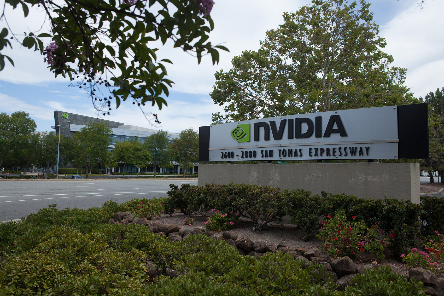
① South Korean media report that NVIDIA is evaluating a glass-substrate solution and collaborating with German equipment manufacturer SCHMID and other companies;
② Currently, the global glass substrate market is accelerating from technology validation to pilot production, customer qualification, and full-scale mass‑production deployment; ③ According to industry analysts, glass core substrates for advanced semiconductor packaging offer vast long-term growth potential.
According to a report by the Seoul Economic Daily, as noted by the STAR Market Daily on September 27,$NVIDIA (NVDA.US)$It is evaluating the adoption of a glass-substrate solution and collaborating with German equipment manufacturer SCHMID and other companies. Additionally, according to South Korean tech media KIPOST, NVIDIA hopes that substrate manufacturers in South Korea, Japan, and Taiwan will complete the development of glass substrates within two years, with potential commercialization as early as before 2028.
 $SCHMID Group (SHMD.US)$At the first-half earnings call, it was disclosed that the company is currently working with…$Intel (INTC.US)$、$NVIDIA (NVDA.US)$、$Advanced Micro Devices (AMD.US)$Collaborating with core suppliers within their respective supply chains, they are jointly developing glass‑substrate equipment. According to Roland Rettenmeier, Chief Strategy Officer at SCHMID, the metallization process for Through‑Glass Vias (TGV) continues to present technical challenges, and customer validation has yet to be completed.
The report states,$NVIDIA (NVDA.US)$CEO Jensen Huang previously met with SK Group Chairman Tae-won Choi to discuss next-generation semiconductor collaborations, including glass substrates, while also actively encouraging Taiwan Semiconductor to develop glass substrate technology. This indicates that NVIDIA is seriously evaluating glass substrate solutions to enhance the performance of its next-generation GPUs.
Earlier in May, NVIDIA and Corning, a leading manufacturer of glass substrates, announced a multi-year strategic partnership: NVIDIA will invest up to $2.7 billion in Corning and receive warrants; in return, Corning will build three advanced manufacturing facilities in the United States, increasing its domestic optical‑connectivity production capacity tenfold to specifically serve hyperscale AI data centers.
Glass substrates are a next-generation semiconductor packaging material, designed to replace traditional organic substrates. As AI chip performance continues to improve, organic substrates are encountering technical bottlenecks such as inadequate thermal resistance and warping. In contrast, glass substrates offer superior flatness and rigidity, enabling chip operating speeds to increase by approximately 40% while reducing power consumption by nearly half.
A low coefficient of thermal expansion is another key advantage of glass substrates, as they exhibit virtually no deformation under high‑temperature conditions—a feature that is especially critical for high‑performance AI chips generating substantial heat. Moreover, glass offers excellent dielectric properties and low signal loss, enabling more reliable transmission of ultra‑high‑speed signals. As substrate dimensions increase, its dimensional stability improves, allowing a single package to accommodate more chips and HBM memory.
Currently, the global glass substrate industry is accelerating its transition from technology validation to pilot-scale production, customer qualification, and mass‑production ramp-up.
Overseas, Intel continues to drive the evolution of Glass Core technology, with DNP, Samsung Electro-Mechanics, LG Innotek, Absolics, and others already in the pilot‑line and customer‑sample stages. Mass‑production milestones are expected around 2028, while material and equipment suppliers such as Corning, AGC, and LPKF are simultaneously working to refine their supporting ecosystems. Domestically, industrialization has also accelerated markedly, with BOE, Vogo Optoelectronics, Mediatek, Lens Technology, and others steadily advancing pilot‑line construction, customer validation, and small‑batch shipments. Meanwhile, domestic supply chains for TGV via‑hole drilling, metallization, RDL, and other processes are gradually being refined.
Huachuang Securities notes that glass core substrates for advanced semiconductor packaging hold vast long-term growth potential. As AI/HPC and HBM drive the expansion of high-end advanced packaging, package sizes are trending toward larger dimensions. The shift toward panel-level packaging is expected to further highlight glass's advantages in large‑size applications, offering superior flatness and reduced warpage. Meanwhile, CPO and high‑frequency RF applications are poised to continue opening up new frontiers.
The institution further noted that, from a supply-chain perspective, domestic production of raw glass substrates remains in its early stages; in the areas of TGV via‑hole formation and glass substrate processing, some Chinese companies have already achieved overseas equipment sales and small‑batch repeat orders; for electroplating and metallization, certain domestic firms have completed delivery and testing of TGV additives and related equipment, begun volume shipments, and are gradually scaling up production; RDL exposure and CMP equipment also warrant close attention.