
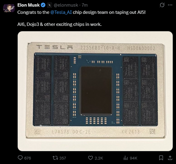
Tesla CEO Elon Musk announced that Tesla's AI chip design team has successfully completed the tape-out of the AI5 chip. This marks a significant milestone in the chip's progress toward the manufacturing stage.
$Tesla (TSLA.US)$ CEO Elon Musk announced that Tesla's AI chip design team has successfully completed the tape-out of the AI5 chip. This marks a significant milestone in moving the chip toward the manufacturing phase. Musk posted on social media, stating, 'Congratulations to Tesla's AI chip design team for completing the AI5 chip tape-out! AI6, Dojo3, and other exciting chips are also in development.' Musk also expressed gratitude to his partners. $Taiwan Semiconductor (TSM.US)$ and Samsung for their support during the mass production process of the chip, stating that "the AI5 chip will become one of the highest-production AI chips globally in the future."
It is reported that the AI5 is Tesla's fifth-generation AI chip, primarily designed for terrestrial applications. Its performance target aims to reach industry-leading levels, matching NVIDIA's Hopper architecture in single-chip configuration and rivaling NVIDIA's Blackwell architecture in dual-chip configuration, while offering lower costs and power consumption. This chip will be integrated into all Tesla vehicle models, future autonomous taxis (Cybercab), and the Optimus humanoid robot, serving as the core of Tesla's terrestrial computing power strategy.
 Musk had previously indicated that the AI5 chip is scheduled to enter mass production in 2027, aiming to replace the AI4 chip currently used in Tesla vehicles. Tape-out is a critical step before mass production of a chip, testing whether the designed chip is functional and preparing it for subsequent large-scale production. The successful tape-out of the AI5 chip signifies a solid step forward toward mass production.
Notably, the A16 chip, which follows the AI5 chip, is currently under development. Musk mentioned last month that the tape-out of the AI6 chip might be completed in December. The iteration cycle between the AI5 and A16 chips is only nine months, whereas the industry-standard chip iteration typically takes over 18 months. With its closed-loop ecosystem of self-developed chips, autonomous driving algorithms, and vehicle manufacturing, Tesla can achieve rapid parameter adjustments and instant feedback from real-world scenarios, significantly compressing the R&D cycle to just nine months.
Tesla’s AI5 and AI6 chips — which will serve as the unified "brain" for millions of autonomous taxis and Optimus humanoid robots — along with the Dojo 3 chip, specifically tailored for the demanding yet highly promising space environment, are important components of Tesla's Terafab superchip factory project officially launched at the end of March. The Terafab project is expected to achieve an annual computational output exceeding 1 terawatt (1TW), equivalent to approximately 50 times the current global annual total computational output of AI chips. Musk has stated that this will be the most ambitious chip manufacturing project in history.
As early as the 2025 shareholder meeting, Musk first clearly outlined the concept of the 'Terafab' chip factory, stating that the existing supplier capacity could not meet future demand, making the construction of a proprietary factory inevitable. Since then, he reiterated the plan multiple times during earnings calls and on social media, emphasizing the decisive significance of chip production to core business operations.
Musk stated that to support the continuous iteration of Tesla’s Full Self-Driving (FSD) software and the large-scale deployment of the Optimus robot, Tesla’s annual demand for chips will reach 100 billion to 200 billion units. Even if global foundries expand production according to the most optimistic forecasts, their capacity would still fall short of Tesla’s explosive demand for AI chips in the future, making the construction of a large-scale wafer fab 'inevitable.'
Musk said, "We are very grateful to our current supply chain, including companies such as Samsung and Taiwan Semiconductor. We hope they can scale up quickly, and we will purchase all the chips they produce. I have already communicated this to them. There is a limit to the pace at which they can expand, but this speed is much slower than our expectations, so we need to build Terafab."
According to estimates, after the Terafab project begins operations, Tesla’s comprehensive chip costs could decrease by 50% to 70%, and its computational energy costs will be only one-third to one-fifth of those of ground-based photovoltaic systems. Product iteration speed will increase two to threefold, greatly enhancing Tesla and its affiliates' cost advantages and technological leadership.
However, entering the semiconductor production field also means that Tesla will face the dual challenges of high investment and high risk. Despite Tesla's cash reserves exceeding $40 billion, the potential total cost of the Terafab project, which could reach tens of billions of dollars, still poses significant financial pressure. Moreover, as an automobile manufacturer, Tesla has no experience in semiconductor manufacturing. Building a wafer fab from scratch using a 2-nanometer process presents multiple challenges, including equipment procurement, talent shortages, and yield control. Therefore, this ambitious plan will subject Tesla to substantial financial and technical challenges.
Currently, the official website for the Terafab project has been launched, and job openings related to Tesla, SpaceX, and xAI have been posted, indicating that the project has entered the substantive advancement stage. Industry analysis suggests that Terafab is not only a crucial step for Tesla in vertically integrating its supply chain but also a significant exploration into the global computing power landscape and the semiconductor industry.
Editor /rice