
CPO chip testing involves three layers of complexity: electrical, optical, and optoelectronic interaction. Currently, there is a lack of unified industry standards, and the process heavily relies on manual operations. The 100% inspection of a single PIC chip takes an average of over 100 seconds. The nanoscale alignment challenge, caused by the nearly 800-fold difference between the cross-sectional areas of optical waveguides and optical fibers, makes CPO testing far more complex than traditional chip testing.
As the expansion of AI data center computing power pushes CPO towards mass production, a previously overlooked link is becoming a bottleneck for the entire industrial chain—testing.
With the continuous expansion of AI data centers, traditional copper interconnects are approaching their physical limits. Co-Packaged Optics (CPO) is regarded by the industry as one of the key interconnection solutions for next-generation AI infrastructure. Taiwan Semiconductor's COUPE platform is expected to enter mass production in 2026, marking CPO's transition from laboratories to commercialization.
 However, the inspection and testing of CPO remains a formidable challenge. The industry currently lacks unified standards, and the process heavily relies on manual operations, making testing one of the main bottlenecks constraining the large-scale mass production of CPO chips. A recent study by TrendForce provides a systematic review of this issue.
Why is CPO testing so difficult?
To understand this question, one must first understand the structure of CPO.
CPO integrates optical components into photonic integrated circuits (PIC), which are then co-packaged with electronic integrated circuits (EIC) into a single chip, using optical paths to replace electrical circuits, thereby reducing power consumption and latency. The component formed after bonding PIC and EIC is called an Optical Engine (OE).
Traditional EIC testing involves purely electrical tests, while PIC contains numerous optical components such as couplers, modulators, photodetectors, optical filters, and optical waveguides. Testing an OE requires expertise in electrical, optical, and optoelectronic interaction aspects simultaneously, making it far more complex than traditional chip testing.
PIC testing requires measuring parameters such as insertion loss (IL), polarization-dependent loss (PDL), responsivity, waveguide propagation loss, and optical crosstalk. Currently, there are no unified testing standards for these parameters.
Another specific physical challenge is the precise alignment of optical probes.
The process of coupling external light from optical fibers into the OE waveguide is called optical coupling. The core cross-sectional area of a single-mode fiber is approximately 78.5 square micrometers, while the waveguide cross-sectional area is only about 0.099 square micrometers—a difference of nearly 800 times. Without nanoscale alignment accuracy, coupling losses will be extremely high.
This means that while maintaining a precise distance from the wafer or chip surface, the fiber array must finely adjust the coupler angle to maximize optical power transmission and then sequentially scan different wavelength ranges. This process currently still relies on manual operation.
The result is that 100% testing of a single PIC chip takes over 100 seconds on average. This is one of the core bottlenecks in the mass production of CPO chips.
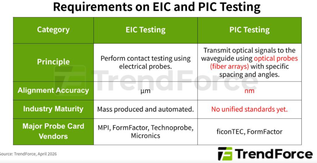
"EIC Testing vs. PIC Testing Comparison Table" — comparing test principles, alignment accuracy, industry maturity, and major probe card manufacturers across four dimensions. Source: TrendForce (same as below).
Among the four testing stages, which step is the most critical?
A CPO chip undergoes four testing stages from wafer to system:
Stage One: PIC Wafer-Level Testing (OWAT) — basic DC electrical and optical testing, including measurements of fundamental optical parameters such as optical power, loss, and dark current.
Stage Two: EIC-PIC Wafer-Level Testing — modulation function testing (electro-optical, optoelectronic, and optical-to-optical), high-speed testing, and S-parameter measurement.
Stage Three: OE-Level Testing — comprehensive calibration, DC testing, high-speed testing, optical loopback testing, and S-parameter measurement. This is the key stage for confirming "Known Good Optical Engines" (KGOE).
Stage Four: Advanced Packaging Module-Level Testing — full-system functional verification and optical loopback testing.
Among the four stages, the first stage, PIC Wafer-Level Testing, is the most critical.
The logic is straightforward: PICs are typically manufactured using mature processes, while EICs rely on advanced processes that are costly. If defective PICs can be screened out at the wafer stage before bonding with EICs, it prevents the wastage of expensive EICs on problematic PICs, significantly reducing losses in subsequent processes.
This is akin to quality control on an assembly line—the earlier problems are detected, the smaller the losses.
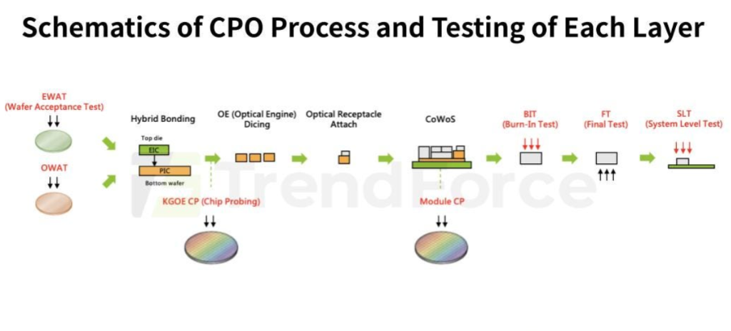
"Schematic Diagram of the CPO Manufacturing Process and Testing Stages"—A complete flowchart from wafer acceptance testing to system-level testing.
Equipment Supplier Landscape: Established Giants Catching Up, New Entrants Joining.
The CPO testing equipment market is rapidly taking shape, with integration between traditional ATE (Automated Test Equipment) giants and optical testing specialists being the main trend.
Advantest and FormFactor
The traditional EIC testing market is dominated by Japan's Advantest ($Advantest (6857.JP)$ ) and the U.S.-based Teradyne ($Teradyne (TER.US)$ ). CPO testing requires both EIC and PIC testing capabilities, and both giants have opted to collaborate with optical probe specialists to address their respective gaps.
Advantest’s approach has been to partner with FormFactor ( $FormFactor (FORM.US)$ ). In June 2024, Advantest, in collaboration with Jenoptik and Ayar Labs, launched the UFO probe card, which integrates electrical and optical probes on a single card to enable synchronized electro-optical testing. Its core innovation lies in alignment tolerance compensation technology—by specially shaping the output beam of the optical probe, even if there are minor positioning errors, the optical signal can still enter the PIC coupler, significantly reducing alignment time.
In April 2025, Advantest and FormFactor further introduced the V93000-Triton photonics testing system, equipped with 9-axis photonics alignment functionality and FormFactor’s OptoVue Pro optical alignment system. Its CalVue technology uses uniquely designed retroreflectors to observe fiber arrays, combined with automated machine vision algorithms for real-time calibration of Z-axis displacement and optical positioning, further compressing fiber alignment times.
Teradyne and ficonTEC
Teradyne adopts a dual approach of acquisitions and collaborations. In 2025, Teradyne acquired Quantifi Photonics and partnered with ficonTEC, a German company now under China's Robo Technik.
In March 2025, the two parties jointly launched the industry's first high-throughput 300mm dual-sided wafer probing test system. ficonTEC provided the WLT-D2 dual-sided wafer testing platform, featuring precision alignment within a 50-nanometer range, enabling simultaneous electrical testing on the top side of the wafer and optical testing on the bottom side to improve testing efficiency. Teradyne contributed the UltraFLEXplus ATE and IG-XL system software.
The subsequently launched DLT-D1 is a dual-sided chip-level testing system capable of connecting up to three parallel test heads simultaneously, increasing throughput and reducing testing costs. With this, ficonTEC has established a complete CPO testing product line ranging from wafer-level to chip-level solutions.
Keysight
Keysight is a global leader in measurement instrumentation, offering a complete PIC wafer testing solution integrated with FormFactor and compatible with FormFactor's Velox probe control software.
Keysight’s N778x series polarization synthesizer enables rapid switching between different states of polarization (SOP), working in conjunction with the N7700100C Polarization Lambda Sweep software to derive parameters such as IL, PDL, and TE/TM IL through matrix methods. This solution eliminates the need for polarization-maintaining fibers and manual pre-calibration of polarization at multiple wavelengths, significantly improving testing efficiency. Its SOP stabilization technology can lock the input light’s polarization state at a specific point, ensuring stable optical coupling throughout the wavelength sweep.
Chroma
Chroma is a global leader in system-level testing (SLT) equipment. Its Model 58604/58604-C/58606 series of photodiode aging and reliability testing systems are specifically designed for reliability testing of PIC components such as 3D sensors, lasers, photodetectors, and modulators. Each module layer of Model 58606 provides 256 SMU channels, configurable up to seven layers for a total of 1,792 channels. Chroma has announced its commitment to leveraging its optical testing expertise in SLT stages to develop CPO testing equipment.
Enlitech
In September 2025, Enlitech collaborated with iST to introduce the Night Jar silicon photonics chip testing platform. This is an add-on hyperspectral imaging analysis system that can be directly mounted on any brand of probe station, suitable for various testing phases including WAT, CP, and FT.
Night Jar addresses a long-standing industry pain point: previously, the location of light leakage in optical waveguides could only be roughly estimated through reflected light, providing only overall or average optical loss values. Night Jar is capable of precisely locating the light leakage positions and measuring the quantified IL values for specific waveguide segments or optical components. It supports wafer-level optical loss mapping, helping researchers identify defects more quickly and accurately, ultimately improving production yield.
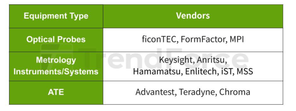
"CPO Testing Equipment Supply Chain Overview" — a distribution map of suppliers across three major categories: optical probes, metrology instruments and systems, and automatic test equipment
The window of market opportunity is opening.
As chip design becomes increasingly complex, the difficulty of SoC testing continues to rise, with the number of test stations required for a single chip and the total testing time constantly increasing. The proportion of testing equipment in semiconductor capital expenditures is therefore rising. With the inclusion of CPO chips into the product portfolio, this proportion is expected to increase further.
The CPO testing equipment market is taking shape. From the perspective of equipment suppliers, traditional automatic test equipment giants Advantest and Teradyne are rapidly enhancing their optical capabilities through acquisitions and collaborations. Meanwhile, companies like Keysight, Chroma, and Enlitech are establishing their positions in respective niche markets. The entire supply chain, from optical probes and metrology instruments to automatic test equipment, is reorganizing around the demands of CPO testing.
Editor/KOKO