
① The Tao (τ) Law proposes replacing “geometric scaling” with “time (τ) scaling” as the new guiding principle for the evolution of semiconductors and electronic systems. ② Based on the Tao (τ) Law, Huawei has already designed and mass-produced 381 chip models. The Kirin chip, set to debut in the fall of 2026, will be the first to adopt Logic Folding technology.
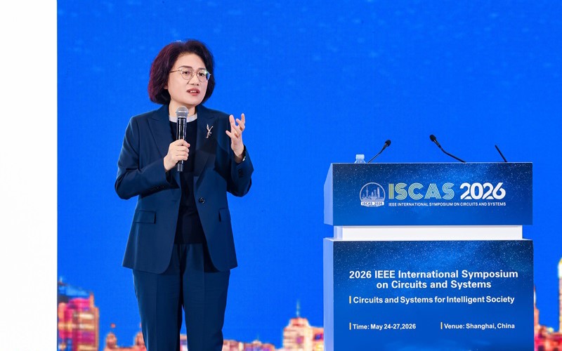
According to a report by The Science and Technology Innovation Board Daily on May 25 (Reporter: Huang Xinyi), today at the IEEE International Symposium on Circuits and Systems (ISCAS 2026), He Tingbo, Director of Huawei’s Board and President of its Semiconductor Business Unit, delivered a keynote speech titled “Exploration and Practice of New Pathways in Semiconductors,” unveiling a new principle for guiding the semiconductor industry—the Tao (τ) Law.
The Tao (τ) Law proposes replacing “geometric scaling” with “time (τ) scaling” as the new guiding principle for the evolution of semiconductors and electronic systems. Its core objective is to systematically reduce the time constant τ through technologies such as Logic Folding, continuously compressing signal propagation delay within chips to further increase transistor density and enable sustained advancement of semiconductors and electronic systems.
 In recent years, Moore’s Law—which has dominated the semiconductor industry for over half a century—has encountered significant challenges stemming from both physical limits and diminishing economic returns. As geometric scaling of transistors slows and cost advantages fade, the industry faces a critical question: how can it transcend the constraints of traditional process pathways and chart a new, sustainable trajectory to meet exponentially growing demands for computational performance? Huawei contends that the Tao (τ) Law offers an effective solution to this challenge.
It is reported that technologies underpinning the Tao (τ) Law, such as Logic Folding, establish a multi-layered framework spanning devices, circuits, chips, and system-level integration.
At the device level, the time constant τ is minimized at the physical foundation by optimizing transistor characteristics and interconnect resistance along with parasitic capacitance.
At the circuit level, Logic Folding transcends the physical limitations of conventional planar layouts, significantly shortening critical path wiring lengths and effectively reducing resistive and capacitive loading on signal propagation, thereby substantially enhancing both transistor density and circuit performance.
At the chip level, full-stack co-design across software, architecture, and silicon enables fine-grained control of instruction and data flows based on actual workloads, improving system-level parallelism and efficiency and drastically reducing end-to-end execution time.
At the system level, the Lingqu Bus is defined to reconstruct interconnect protocols within computing systems, enabling unified memory addressing and native memory semantics across supernodes, thereby significantly lowering system communication latency.
In summary, this framework can be understood as follows: under constraints on transistor density, the Tao (τ) Law optimizes and shortens signal transmission and processing times—from底层 devices to top-level systems—to enhance chip performance and energy efficiency.
In this keynote speech, He Tingbo explained Huawei's practical application of Tao's Law (τ Law) in the fields of smartphones and AI computing. Based on Tao's Law, Huawei has already designed and mass-produced 381 chip models.
Among these, the Kirin chip set to launch in the fall of 2026 will be the first to adopt logic folding technology, significantly enhancing performance. By 2031, high-end chips based on Tao's Law are expected to achieve transistor density equivalent to that of a 1.4-nanometer process node.
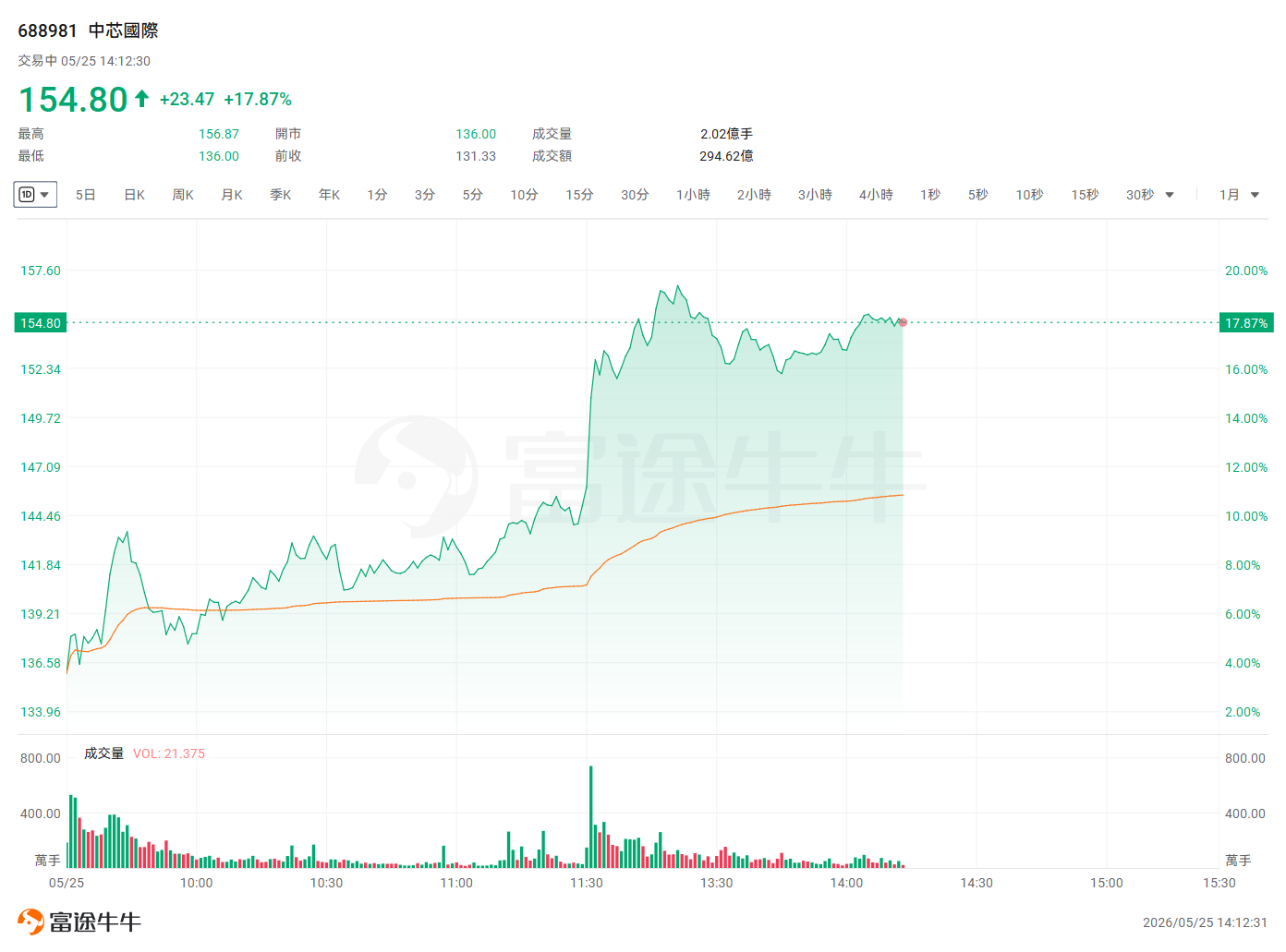
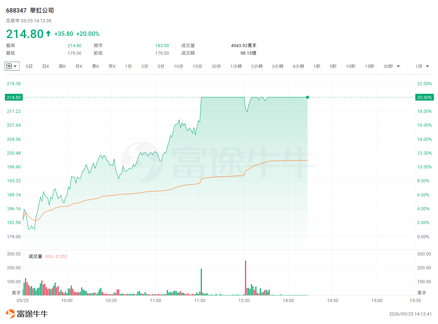
After He Tingbo announced the above information, $Semiconductor Manufacturing International Corporation (688981.SH)$ its share price on the A-share market rose by more than 19%, $Hua Hong Semiconductor (688347.SH)$ surged by the daily trading limit of 20%.
Huawei introduced 'Tao's Law' at a critical inflection point when Moore's Law—the long-standing principle guiding the semiconductor industry—has begun to lose its validity.
In 1965, Gordon Moore, co-founder of Intel, observed from integrated circuit development data between 1958 and 1965 that the number of transistors and other components on a chip doubled annually. He predicted this rapid growth trend would continue for another decade—an observation later widely recognized in the industry as 'Moore's Law.' As the semiconductor industry evolved rapidly, Moore revised the doubling cycle to every two years in 1975. Subsequently, considering the combined pace of improvements in chip performance and operating frequency, the industry gradually adopted an 18-month iteration cycle as the standard benchmark for semiconductor development over the following decades.
However, as transistor scaling approaches physical limits, the driving force behind Moore's Law has significantly weakened. The industry has shifted toward new approaches such as novel chip architectures, 3D packaging, and chiplets to continue advancing transistor density and chip performance. In this transition, several industry leaders have proposed their own new 'laws.' Among them,$NVIDIA (NVDA.US)$NVIDIA CEO Jensen Huang’s widely cited 'Huang’s Law' states that AI chip computational performance improves by a factor of 1,000 every decade—a pace far exceeding that of traditional Moore’s Law.
Amid the waning influence of Moore’s Law and the emergence of competing new paradigms, whether Tao’s Law can truly become the dominant framework in the post-Moore era remains to be validated over time by the market and the broader semiconductor supply chain. Nevertheless, Huawei’s proactive effort to define new rules through large-scale implementation undoubtedly offers the global semiconductor industry a Chinese pathway worthy of close attention.
Editor/Rocky