
Huawei has unveiled its "tau scaling" technology framework, shifting the core metric for chip performance from "nanometer process nodes" to "system latency optimization." This approach leverages co-optimization across packaging, interconnects, memory, and architecture to address the physical limitations of geometric scaling. Huawei is pivoting its focus from single-node miniaturization toward system-level integration, potentially creating strategic revaluation and scale-up validation opportunities across key segments of the supply chain, including advanced packaging, 3D design, and interconnect memory technologies.
Huawei has reframed the narrative around chip performance improvement. Historically, the industry’s most common benchmark was who could advance to more advanced process nodes faster; this time, 'tau scaling' shifts the yardstick from 'how many nanometers' to 'how much time.' Transistor switching, signal propagation, compute-memory access, and system-level communication are all now incorporated into a unified time-optimization framework.
On May 25, He Tingbo, Head of Huawei Semiconductors, published a signed paper detailing Huawei’s widely discussed new chip technology. Its core thesis can be summarized in one sentence: Process nodes have not exited the stage, but packaging, interconnects, memory bandwidth, protocol stacks, and system architecture—factors beyond the node—are now being pushed to the forefront.
 Huawei simultaneously disclosed three key data points: Over the past six years, it has designed and mass-produced 381 chips based on this methodology; its next-generation Kirin chip, launching this fall, will adopt LogicFolding for the first time; and by 2031, high-end chips developed along this roadmap will achieve transistor density equivalent to that of a 1.4-nanometer process node.
The implications of this approach extend beyond smartphone chips. On mobile devices, the focus is on compressing latency within a single SoC; on AI systems, it centers on communication delays among thousands of chips. What the market should truly monitor is not just the benchmark scores of the next-generation Kirin, but whether advanced packaging, hybrid bonding, 3D design tools, memory-logic co-design, and system interconnects will enter phases of validation and scale-up.
Process nodes haven’t exited the stage—but relying solely on nodes is no longer sufficient to explain performance gains.
For decades, the semiconductor industry followed a straightforward trajectory: smaller transistors meant more devices per unit area, higher frequencies, and—over an extended period—lower power consumption and cost per transistor. Consequently, advanced process nodes became the hardest metric in the performance race.
Tau scaling addresses a different layer of the problem: even if transistors continue to shrink, a significant portion of time consumption on a chip does not stem from the transistors themselves. It takes time for signals to travel from one end of the chip to the other, for compute units to wait for data, and for chips to communicate with each other. Geometric scaling solves 'making things smaller,' while tau scaling aims to solve 'running faster and waiting less.'
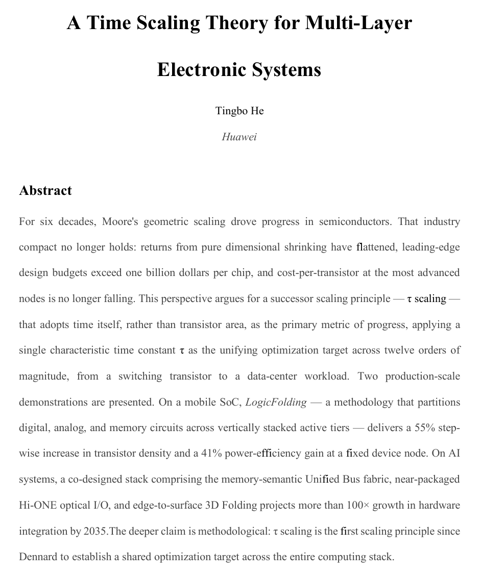
Huawei’s framework spans four layers: devices, circuits, chips, and systems. Rather than optimizing a single circuit module, it integrates latency across all levels into a unified optimization objective. In terms of the supply chain, this means value creation will no longer concentrate solely on front-end manufacturing; packaging, interconnects, memory, and system architecture will all assume greater weight.
This is precisely where 'replacing geometric scaling with time-based scaling' matters most. 'Replacement' does not mean advanced process nodes are unnecessary; rather, it means performance improvements can no longer rely exclusively on the next-generation node.
LogicFolding: A Kirin Breakthrough at a Fixed Node
The most compelling engineering demonstration of tau scaling is the Kirin 2026, which will enter mass production this autumn.
The design philosophy behind LogicFolding is to break down the physical boundaries of traditional planar layouts by splitting digital, analog, and memory circuits across multiple vertically stacked active layers, interconnected via ultra-fine-pitch hybrid bonding to significantly shorten signal propagation distances along critical paths.
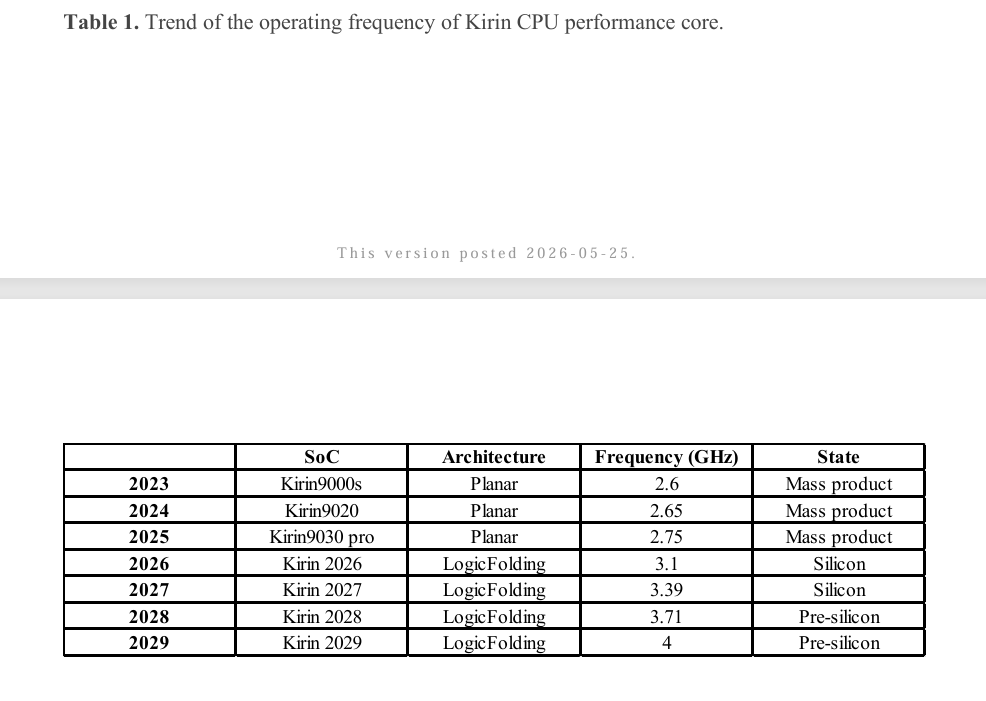
Measurement results show that transistor density within a single-generation product has increased from 155 million transistors per square millimeter to 238 million—a 55% gain—equivalent to the advancement traditionally achievable only through three years of geometric scaling. The SoC’s performance-core power efficiency improved by 41%, peak clock frequency rose by nearly 13%, and the CPU’s main core frequency returned to 3.1 GHz. On the SRAM side, operating frequency increased by over 40%. In representative processor cores, clock buffer count decreased by more than 50%, clock skew was reduced by 25%, and interconnect length shortened by approximately 30%.
Huawei described the implemented version of the Kirin 2026 as 'deliberately conservative': hybrid bonding pitch was set at 1.5 micrometers, and folding was selectively applied only along critical paths. According to its roadmap, the Kirin series’ CPU clock frequency is projected to reach 3.39 GHz in 2027, 3.71 GHz in 2028, and surpass 4 GHz in 2029. Transistor density is expected to exceed 400 million per square millimeter by 2031, equivalent to the level of a 1.4-nanometer process node. In her paper, He Tingbo characterized this roadmap as 'feasible and economically viable in terms of cost.'
This is not about 'bypassing lithography tools,' but rather about disaggregating performance gains and seeking them elsewhere.
Interpreting tau scaling as 'bypassing lithography tools' misrepresents the issue. Huawei’s public statements arise from the context that geometric scaling is increasingly approaching physical limits, and its cost-benefit ratio is weakening; thus, further performance improvements can no longer rely solely on more advanced process nodes.
This means that advanced process nodes remain important, but they are no longer the sole variable. Internal circuit efficiency, data movement distance, memory access speed, and system communication latency may all become new sources of performance gains.
In other words, the industry’s most pressing question used to be: 'Who gets access to the next-generation node first?' Now, an additional question must be asked: Who can seamlessly integrate nodes, packaging, interconnects, memory, and system architecture?
This shift will reshape supply chain roles. Technologies previously viewed as ancillary—such as advanced packaging, hybrid bonding, 3D toolchains, memory interfaces, and system interconnects—are now assuming greater centrality. They are no longer merely about 'packaging chips' or 'connecting chips,' but directly contribute to performance enhancement.
The bottleneck in AI systems resembles a 'timing problem' more closely than it does in smartphones.
Mobile phone chips address timing within a single chip, whereas AI systems address timing across a group—or even an entire rack—of chips. The larger the model and the greater the scale of computing power, the more pronounced the cost of moving data between chips, memory, and interconnect networks becomes.
The UnifiedBus mentioned in Huawei’s public framework aims to unify memory addressing and native memory semantics to reduce system communication latency. It targets not the performance of a single chip, but the efficiency of data scheduling at the system level.
Applying this logic to systems like SuperPoD clarifies the direction: accelerating individual chips is merely the first step; the greater performance gains may come from reducing latency across the entire computing system. In AI computing, the bottleneck often lies not in whether compute power exists, but in whether that compute power can access data in time.
This is also where τ scaling holds greater potential in AI scenarios. As long as data movement and communication wait times constitute a sufficiently large share of total execution time, system-level optimizations could yield more significant benefits than incremental improvements in process technology alone.
What the market needs to see is not just concepts, but three rounds of tangible validation.
With the roadmap now on the table, market attention will quickly shift toward actual implementation and validation.
The mass production of the Kirin chip in autumn 2026 will serve as the first externally verifiable milestone for the τ scaling roadmap: the amount of independently verifiable performance and energy efficiency data delivered by LogicFolding in a mass-produced product will constitute the first public test of this framework’s credibility. Second, it will matter whether Huawei further discloses its complete methodology and engineering details to foster broader industry collaboration. Third, responses from the supply chain—such as capacity expansion plans, order trends, and customer validations in advanced packaging, hybrid bonding, and 3D toolchain development—will be critical signals indicating whether this roadmap can evolve into an industry-wide consensus.
From the current point to 2035, the full validation of τ scaling spans three levels: optimizing intra-chip timing on the mobile side, optimizing inter-chip timing across thousands or even tens of thousands of chips on the AI side, and shifting value creation on the industrial side from front-end manufacturing toward packaging, interconnects, and system architecture. The roadmap’s direction has been set; the gradual realization through products and the supply chain will be the core pricing variable over the coming years.
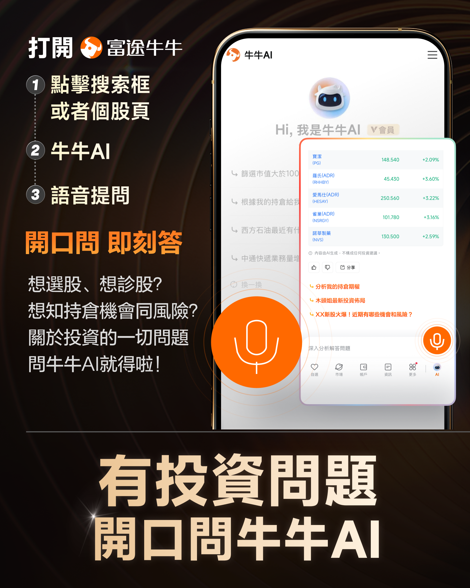
 Looking to pick stocks or analyze them? Want to know the opportunities and risks in your portfolio? For all your investment-related questions,just ask Futubull AI!
Editor/KOKO