
Objectively assess
The hottest topic today is a single letter: τ.
He Tingbo, President of Huawei’s Semiconductor Business, formally introduced a new concept—the “Tao (τ) Law”—at the International Conference on Circuits and Systems.
 This marks the first time a Chinese company has proposed a new principle to guide the entire global semiconductor industry.
Can it truly align with the current state of the chip industry and replace Moore’s Law as the core industry doctrine for the next decade?
01
Since Gordon Moore first articulated Moore’s Law in 1965, the foundational logic of the semiconductor industry has been straightforward and aggressive: geometric scaling.
In simple terms, this means making transistors smaller and smaller. Every 18 to 24 months, the number of transistors on a chip of the same area doubles, performance doubles, and cost halves.
But from 90 nanometers and 28 nanometers all the way to today’s 3-nanometer and 2-nanometer nodes, this approach has inevitably run into two fundamental barriers:
Physical limits
The diameter of a silicon atom is approximately 0.22 nanometers, and the lattice spacing is about 0.54 nanometers.
When the manufacturing process approaches 2 nanometers or even 1 nanometer, it is no longer engineering—it’s 'sculpting atoms.'
At this point, a physical phenomenon that still lacks a complete explanation emerges: quantum tunneling.
When the transistor gates that control electric current become only a few atoms thick, electrons can 'leak' through them as if passing through walls. The switches can no longer block the flow, causing current to run rampant—resulting directly in extremely severe leakage and heat generation.
As early as 2005, Dennard scaling—which once paralleled Moore’s Law—was declared obsolete, ushering the semiconductor industry into the painful 'dark silicon era.'
Although more transistors can be packed onto a chip, you cannot afford to turn them all on simultaneously—because the chip would melt instantly.
Economic Limits
Behind Moore’s Law lies another often-overlooked principle known as Rock’s Law, which states that the cost of semiconductor fabrication plants doubles every four years.
According to Taiwan Semiconductor’s annual financial reports and industry estimates, building a 28-nanometer wafer fabrication facility costs approximately USD 6 billion; by the time the industry reached the 3-nanometer node, that figure had surged to at least USD 20 billion.
The more advanced the technology becomes, the fewer players can afford to stay in the game.
Twenty years ago, dozens of world-class wafer fabs operated globally. Today? Only three remain at the table: Taiwan Semiconductor, Samsung, and Intel.
The cost benefits of transistors have long since entirely disappeared, and the marginal returns from scaling have plummeted dramatically.
On the demand side, however, as the AI arms race intensifies, demand is surging exponentially.
On one side is the painstakingly slow and extremely costly 'geometric scaling'; on the other is insatiable demand for computing power.
This enormous divergence—this 'scissors gap'—represents the market's most pressing pain point today.
One potential solution is Tao’s Law (τ Law), centered on replacing 'geometric scaling' with 'temporal scaling'—scaling in time (τ).
Here, the Greek letter τ represents the 'time constant.'
In circuits, it primarily refers to RC delay (resistance-capacitance delay)—the time required for a signal to travel from point A to point B in a circuit and complete a state transition.
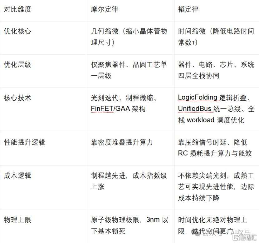
Moore’s Law operates in the 'spatial dimension': to enhance performance, transistors must be made smaller and denser, and interconnects thinner, thereby packing more data into a given area.
Tao’s Law operates in the 'temporal dimension': rather than relentlessly shrinking transistors, it systematically reduces the time constant τ. The goal is to enable signals to move faster, travel shorter distances, and wait less within the system.
To illustrate:
Beijing’s morning rush-hour traffic jams are addressed by Moore’s Law through inventing narrower micro-cars that can be squeezed into the Second Ring Road.
Tao’s Law tackles the problem by “optimizing traffic light systems, constructing 3D elevated interchanges, building subways, and implementing tidal lanes.” Without changing vehicle size, commuting time is drastically reduced, achieving a leap in the city’s overall traffic throughput (performance).
If Moore’s Law represents the art of micro-sculpture—building skyscrapers on the tip of a needle—then Tao’s Law embodies system-level urban planning that eliminates citywide traffic congestion.
At its core, this is a thought experiment rather than a technological revolution.
02
To achieve “time scaling,” a coordinated optimization framework spanning four hierarchical levels must be established.
1. Device Level
Since aggressive scaling to a few nanometers is not required, engineers can adopt new materials (such as backside power delivery networks and novel contact materials) to minimize the device-level time constant τ at the foundational layer.
2. Circuit Level
By transcending the physical constraints of planar layouts, logic circuits previously laid out on a two-dimensional plane can be folded into three-dimensional space using 3D stacking technology.
Two modules that were originally far apart can now be brought significantly closer after folding, directly reducing the wiring length of critical paths and thereby lowering resistive and capacitive signal propagation loads.
3. Chip Level
In the past, chip design was a black box—software engineers did not concern themselves with how hardware operated.
Tao’s Law mandates full-stack co-design across 'software, architecture, and chips,' enabling fine-grained control over instruction and data flows based on actual workloads. Algorithms are leveraged to enhance system parallelism and minimize idle waiting time, thereby significantly reducing end-to-end execution latency.
4. System Level
In simple terms, hundreds of AI accelerator cards are interconnected via the Lingqu bus, appearing to software as a single super card with virtually unlimited memory capacity.
Communication latency is drastically compressed, and the time constant is substantially reduced at the system level.
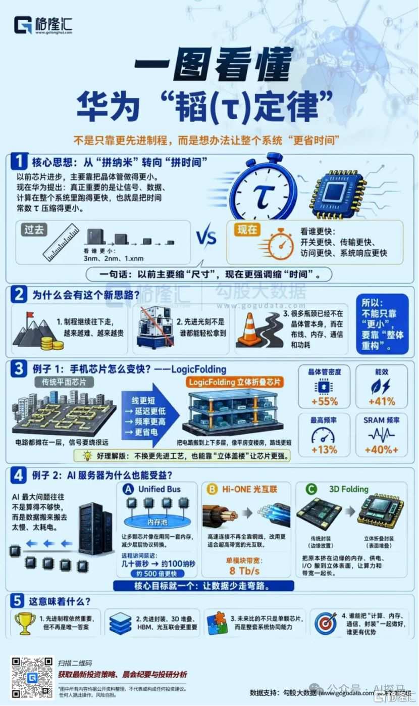
This represents the first new theoretical framework in the global semiconductor industry—since the breakdown of Dennard scaling—to establish a unified optimization objective across the entire computing stack.
Its greatest strategic advantage is clear: bypassing reliance on advanced photolithography and overcoming critical supply chain bottlenecks.
It delivers performance comparable to advanced process nodes using hardware built on mature manufacturing processes.
However, despite all this, many may still feel that these statements merely articulate goals without offering concrete, actionable proposals.
No matter how you argue it, 2nm is objectively superior to 3nm—that’s an indisputable fact.
Perhaps to alleviate skepticism and demonstrate that Tao’s Law is not mere speculation, CEO He pledged that the new Kirin chip to be launched this autumn will fully and率先 adopt 'logic folding technology,' expanding from a single layer to dual layers.
He also set an ambitious target: without relying on the most advanced extreme ultraviolet (EUV) lithography machines, achieve by 2031 a transistor density in high-end chips equivalent to that of a 1.4 nm process node.
However, achieving this goal is undoubtedly extremely difficult.
Do not blindly praise it—Tao’s Law has undeniable shortcomings.
First, the design complexity is too high. Logic folding not only increases routing difficulty but also poses significant thermal challenges. With logic layers stacked together, how can heat be effectively dissipated? This places exceptionally high demands on materials science and thermal management.
Second, there are no established industry standards. Moore’s Law benefits from mature EDA toolkits; Tao’s Law, with its entirely new architecture, requires rebuilding many simulation tools and test standards from the ground up.
Even if HW can overcome these difficulties, there remains another issue.
This approach requires seamless integration from foundational components and chip architecture all the way up to the operating system and bus protocols, representing a closed-loop, in-house technology ecosystem developed by Huawei.
Globally, aside from Apple, there is virtually no third company capable of maintaining full control over all four layers of this full-stack stack.
In other words, Tao's Law lacks universality due to excessively high ecosystem barriers.
If that is the case, its impact on the entire industry may not be as significant as imagined.
03
In fact, looking globally, all manufacturers are indirectly seeking alternatives to Moore's Law.
Taiwan Semiconductor’s CoWoS, Intel’s Foveros, and AMD’s 3D V-Cache are all pursuing similar approaches aimed at shortening communication distances and improving system efficiency.
However, to date, no one has claimed to have found a perfect solution to the challenges posed by Moore's Law.
Either the technical difficulty is too high, or the solution lacks broad applicability.
At least for now, IP design, EDA tools, wafer fabrication, and packaging/testing based on Moore’s Law have already formed a perfectly closed loop.
Although its drawbacks are now evident, it remains the most cost-effective solution available.
Of course, this does not negate breakthrough innovation.
For example, Tao’s Law emphasizes speed in time and high efficiency rather than blindly pursuing physical 'smallness.'
Regardless of success or failure, it is a great attempt. (End of article)
Editor/melody