
Intel CEO Lip-Bu Tan has set a goal of achieving a tenfold return within five to ten years, systematically redefining the company’s technology roadmap by advancing EMIB (Embedded Multi-die Interconnect Bridge) packaging, glass substrates, and new materials such as synthetic diamond to overcome physical limits. The surge in AI agent adoption is driving a strong rebound in CPU demand; the foundry business will prioritize yield and trust, collaborating with Elon Musk on the Terafab project, with Intel’s full potential expected to materialize after 2030.
$Intel (INTC.US)$CEO Lip-Bu Tan stated that his return target for Intel is "a tenfold increase within five to ten years," and he is systematically restructuring Intel's technology roadmap around advanced packaging, novel semiconductor materials, and next-generation substrate technologies.
In a recent podcast episode, Tan elaborated on his strategy for transforming Intel: after stabilizing the balance sheet and streamlining the product portfolio, he is now focusing investments on advanced packaging technology EMIB, glass substrates, and new materials such as gallium nitride (GaN), silicon carbide (SiC), indium phosphide (InP), and synthetic diamond to address the challenges posed by the physical limits of traditional process node scaling. He also noted that the surge in agent AI and inference workloads is driving a strong rebound in CPU demand, with the CPU-to-GPU ratio in data center servers shifting from the historical 1:8 toward 1:4 or even lower.
 Tan said that Intel has already delivered approximately a sixfold return to shareholders over the past 14 months, but "this is just the beginning." He expects that by 2030–2032, the market will begin to fully recognize Intel’s potential—not only in its traditional PC client business but also in emerging markets such as edge computing, physical AI, and agent AI.
In his view, if Intel can effectively integrate its XPU strategy, advanced packaging capabilities, and foundry services, it will be able to deliver customized chip solutions for diverse workloads—a long-term strategic direction he has set for the company.
New materials are key to breaking through; advanced packaging and glass substrates are central priorities
As traditional process node scaling increasingly approaches physical limits, Tan has identified materials science and advanced packaging as critical breakthrough areas. He noted that Intel is already mass-producing its 18A process node, advancing toward 14A production, and can envision a technology path down to 10 nanometers and even 7 nanometers—but "this path will become increasingly expensive and difficult."
To this end, Tan has initiated multiple strategic moves in packaging materials. He has invested in glass substrate company 3DGS, attracted by glass’s unique thermal and insulating properties. In interconnect technology, Intel is championing its next-generation advanced packaging solution EMIB and has announced advanced packaging manufacturing collaborations in India and New Mexico, USA. With approximately 1,000 patents in module technology, Tan emphasized that effectively integrating substrates with modules is a core engineering challenge.
In the area of novel semiconductor materials, Tan said Intel has made investments across gallium nitride, silicon carbide, and indium phosphide—some of which have already been acquired by major semiconductor firms like Analog Devices (ADI). He has also invested in a synthetic diamond wafer company, citing diamond’s promising potential as a thermal management material in chip packaging. “That’s the engineer’s mindset—you keep hitting bottlenecks, and then you figure out how to overcome or circumvent them,” he said.
Foundry Business: Trust Comes First; Yield and Cycle Time Are Core Metrics
$Intel (INTC.US)$The foundry business was once viewed externally as unsustainable, but Tan chose to stay the course. He explained that the core rationale behind this decision is that advanced domestic manufacturing in the United States holds strategic value for supply chain security, and no major semiconductor company can afford to concentrate its supply chain heavily in just one or two geographic regions.
At the execution level, Lip-Bu Tan has identified yield, defect density, and cycle time as the key performance indicators for Intel’s foundry business. He emphasized that foundry is fundamentally a trust-based business—'Customers must trust you before they hand over their wafers.' Once yield falls short of expectations, customer attrition due to lost revenue becomes difficult to reverse.
He also stated that Intel and Taiwan Semiconductor maintain a partnership rather than a purely competitive relationship, and that the industry as a whole needs additional capacity to meet continuously growing demand. He expects Intel’s foundry business to begin demonstrating its true potential in the market between 2030 and 2032.
Terafab Collaboration: Building Semiconductor Infrastructure with Elon Musk
Tan revealed that$Intel (INTC.US)$the Terafab project with Elon Musk originated from their shared assessment that semiconductor infrastructure development has lagged behind the growth of AI demand in terms of capacity, production efficiency, and power efficiency. Under this collaboration framework, Musk decided to build his own wafer fabrication facility, and Intel will provide technological and process support to help accelerate production ramp-up. Tan noted that he holds weekly meetings with Musk’s team and that the collaboration is progressing smoothly.
He also mentioned that Musk brings unconventional operational thinking—for example, they once discussed whether smoking should be permitted in certain areas of the cleanroom. 'I might not go that far, but perhaps it could be allowed in some zones—the key is maintaining an open mindset.'
Investors’ Biggest Misconception: Intel Is Still in the 'Crawling' Phase; True Potential to Emerge After 2030
In response to market skepticism regarding$Intel (INTC.US)$the pace of transformation, Tan invoked his longstanding “crawl-walk-run” framework. He explained that the past several months have still been in the “crawl” phase: Intel is quietly building out its CPU architecture, GPU architecture, and software architecture teams and striving to drive breakthrough innovation at the speed of a “large startup.” On the foundry side, the gap with Taiwan Semiconductor remains significant, and Intel must remain humble while strengthening foundational capabilities such as intellectual property and yield.
"My venture capital instincts tell me—to seek 10x return opportunities," said Lip-Bu Tan. Citing his experience at Cadence as a reference—from serving as interim CEO to stepping down—he generated approximately 76x to 85x returns for shareholders. He acknowledged that Intel’s scale makes replication more challenging, but achieving 'a 10x return within five to ten years' remains his clearly defined personal goal.
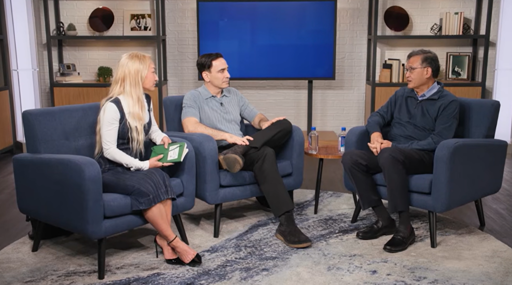
Below is the full transcript of the interview:
Host: Welcome back to No Priors. Today, Allad and I are joined by Lip-Bu Tan—a legendary investor from Walden, former CEO of Cadence, and current CEO of Intel. We’ll discuss his plan to transform Intel, what it means for the U.S. government to become a major shareholder, how to be an exceptional semiconductor investor, and whether we can manufacture chips domestically in the United States. Welcome, Lip-Bu.
Why did you take on the challenge of leading Intel?
Moderator: Let’s start with an obvious question. Becoming CEO of this critically important U.S. semiconductor company is an exceptionally difficult job. Why did you take it?
Lip-Bu Tan: That’s a good question. I’m 66 years old, and many people say I should retire—why take on the most challenging role in the industry? There are several reasons: First, this is an iconic company, vitally important to the entire semiconductor ecosystem and to the United States. Second, after Cadence, I decided I wanted to do one more big thing.
Moderator: A lot has happened over the past year. What surprised you the most?
Lip-Bu Tan: The most surprising event was something I had never encountered in any prior job or training—early one morning, President Trump asked me to resign, citing a conflict of interest with no exceptions allowed. At first, I had to convince myself: I don’t need this job; I’m doing this purely to save Intel. Once I set aside my personal feelings, I began thinking about what I could do for Intel. Fortunately, I secured a meeting that Thursday morning, followed by another on Monday. I presented my case—hearing that I was born in Malaysia, raised in Singapore, graduated from MIT, and have lived in the U.S. ever since without leaving. He listened, understood, and gave me the opportunity to continue. I’m deeply grateful.
Moderator: You described this role as 'saving Intel.' What does success look like for Intel in your mind—what would a thriving Intel look like?
Lip-Bu Tan: It’s been 14 months, and a great deal has happened. First, we’re transforming the culture—establishing clear accountability and accelerating decision-making. I’m accustomed to the pace of startups, where everything moves at light speed, but Intel had layer upon layer of bureaucratic meetings, which I needed to change. Second, we’re listening to our customers—you must be humble, willing to listen, confront their challenges directly, and solve them. Third, from day one, I decided that all engineering teams would report directly to me. As an engineer by training, I need to know firsthand where problems exist and what requires correction. Listening to customers, satisfying their needs, ensuring we have the right products, streamlining our product portfolio, and establishing a clear roadmap and vision for the next five to ten years—these are our priorities.
Intel’s Ten-Year Vision
Moderator: What is your vision for Intel ten years from now?
Lip-Bu Tan: My consistent approach—whether at Cadence or Intel—is to first crawl: stay humble and listen to customers; then walk; and eventually run. One step at a time.
The first step is strengthening the balance sheet—to be honest, its condition was quite poor at the time. I’m pleased that the U.S. government has become a major shareholder. I explained to President Trump: Look at Japan, look at Singapore—this is infrastructure-level support, and governments should rightfully provide it.
Second, I am deeply grateful to my longtime friend Jensen Huang—he invested $5 billion in Intel, and I’m pleased that my efforts have added significant value; his $5 billion has now grown to $25 billion or more. Additionally, Masayoshi Son of SoftBank—who I served with on SoftBank’s board—also stepped in to help. Through these actions, we have strengthened our balance sheet.
Next is focusing on products, streamlining the product portfolio, listening closely to customers, and launching next-generation leading-edge products. It so happens that demand for AI agents and inference CPUs is extremely strong right now, so in a sense, I’ve caught a favorable wave. Historically, the CPU-to-GPU ratio during training was roughly 1:8, but I now see it shifting to 1:4 or even lower. CPUs are becoming more important, which gives me great satisfaction.
I’ve spoken with several AI model developers who told me that CPUs actually perform better in reinforcement learning phases and in coordinating and scheduling the speed of all agents. As a result, demand for my CPUs is currently very high. After establishing a solid foundation in our data center server product line, another critical business area is our wafer foundry operations. This is a capital-intensive business and not easy to execute. You need the right mix of IP—for example, low-power IP for mobile clients—and without it, you simply can’t serve them. It’s a service business and also a trust-based business—if yields fall short, customers will abandon you due to revenue losses. Therefore, I am intensely focused on yield, defect density, and cycle time to ensure we deliver high quality and reliability to our customers. Ultimately, we must move toward a full-stack offering—not just silicon itself. You need software; some customers come directly to me asking, ‘Give me an entire rack,’ so you must provide system-level solutions. I am quietly advancing all these initiatives step by step while recruiting the best talent I can find. By the way, I personally handle all hiring myself—I don’t use any executive search firms.
Collaborating with Elon Musk on Terafab
Moderator: Another widely discussed strategic initiative is Terafab and your collaboration with Elon Musk. Could you share how this partnership came about and how you work together?
Lip-Bu Tan: I believe we both agree that Elon Musk is one of the greatest entrepreneurs of this century. He and I share a common assessment: semiconductor infrastructure has not kept pace with the growth of AI—there are gaps in capacity, manufacturing efficiency, and power efficiency, and we both recognize this challenge.
Second, I truly enjoy working with him. He is highly unconventional and constantly questions every step by asking, ‘Why do it the traditional way?’—which is refreshingly innovative. I welcome diverse perspectives and enjoy collaboratively identifying the optimal path forward, where both sides learn a great deal. He has a clear vision—his robots and vehicles require vast quantities of chips.
Specifically regarding Terafab, he decided to build his own wafer fabrication facility, and we are eager to collaborate with him to accelerate production by leveraging some of our technologies and processes—this is a joint effort. His team is excellent; I meet with them weekly, and working with him is truly inspiring. He has floated unconventional ideas, such as allowing smoking inside cleanrooms—a practice I might not adopt fully, but perhaps certain designated areas could be considered. The key is maintaining an open mindset, and we are carefully listening to and evaluating his suggestions.
The Evolving Global Semiconductor Supply Chain
Moderator: Looking at the macro landscape, how do you observe AI reshaping the global semiconductor supply chain on a country-by-country basis?
Lip-Bu Tan: AI’s impact on the overall landscape will surpass that of the internet, and its influence will be even more profound. AI first enables you to accomplish tasks more efficiently. With the assistance of numerous intelligent agents, many tedious tasks that previously required manual effort can now be completed much faster. For instance, in semiconductor design, timing optimization and time-to-market can both be significantly improved, while costs can also be reduced.
AI demand growth faces several bottlenecks: First is power constraints—some countries simply do not have sufficient electricity. Second is the impact of helium gas, which many people fail to recognize as having a significant effect on the semiconductor industry. Third is memory shortages, which currently represent the most urgent issue—even if new capacity is added today, it will take several years before that capacity comes online. CPUs and GPUs are similarly in short supply, driving up prices, with costs ultimately passed on to end customers.
The companies most severely impacted will be those that fail to embrace AI. AI can help enterprises enhance efficiency across virtually all functional areas. Companies should proactively adopt AI and identify better ways to leverage it—whether for forecasting, design, or various workloads.
Moderator: The simplest argument against Terafab and Intel Foundry’s competitiveness centers on labor costs and the feasibility of domestic manufacturing. What is the rationale behind your decision to further double down on foundry business?
Lip-Bu Tan: When I was deciding whether to continue betting on foundry services or exit the business, there was a lot of external commentary—various voices claiming it was too expensive or unworkable. But I ultimately concluded that this is critically important for the United States and for the entire industry.
We have all experienced supply chain challenges. Any major semiconductor company must seriously consider its supply chain strategy and ensure it has a robust and resilient supply chain, without overreliance on just one or two geographically concentrated suppliers. An increasing number of stakeholders will recognize that domestic manufacturing in the U.S. is essential.
Our most advanced process nodes, such as 18A—which corresponds to the 1.4-nanometer class—are already being developed further; we are planning for 1-nanometer and even 0.7-nanometer technologies. As process nodes shrink ever smaller, line widths become finer than a human hair, and complexity increases dramatically. A single error at any step could jeopardize the entire effort. Precisely because of this, manufacturing precision requirements are rising continuously, and this will increasingly become a bottleneck.
We hold Taiwan Semiconductor in very high regard—they are an excellent partner. Moreover, the industry needs additional capacity to serve customers effectively, so we decided to persevere despite the challenges. In the long run, this is a pivotal move and represents where I can create the greatest value for the industry.
Physical Limits and Advanced Packaging
Moderator: People have long debated that chip scaling will eventually hit physical limits—when line widths become too narrow, further miniaturization becomes impossible. When do you think we will truly reach that wall?
Lip-Bu Tan: We currently have 18A, and we are advancing the mass production of 14A. I can see a clear path toward 10-nanometer and 7-nanometer nodes—this path is achievable, but it will become increasingly expensive and challenging. This is precisely why we need partners and must collaborate closely with substrate suppliers and equipment manufacturers to jointly drive improvements in yield and performance.
Another critical area that is becoming a bottleneck is advanced packaging. Taiwan Semiconductor has CoWoS, and we have a next-generation solution called EMIB. I must ensure it achieves the yield required by customers during mass production.
As traditional scaling begins to hit bottlenecks, I’ve started looking for breakthroughs at the materials level—gallium nitride, silicon carbide, and indium phosphide. I’ve invested in all three directions. In packaging materials, I’m now focusing on glass—glass is an excellent thermal insulator, and I’ve invested in a company called 3DGS. Intel holds approximately 1,000 patents related to modules, and integrating substrates with modules is a key challenge. We recently announced new advanced packaging manufacturing collaborations in India and New Mexico, USA. Additionally, I’m also exploring synthetic diamond—an exceptional thermal insulating material—and have invested in a diamond wafer company.
That’s the engineer’s spirit—you keep running into bottlenecks, and then you figure out how to overcome or bypass them. Having been deeply involved across the entire semiconductor lifecycle—from EDA tools to design and manufacturing—I’m now delighted to apply this experience to contribute meaningfully to the industry.
Moderator: Could there be a scenario where process node convergence narrows the performance gap between different foundries, leading to some kind of asymptotic limit?
Lip-Bu Tan: The essence of Moore’s Law is doubling transistor density, but power consumption and cost do not decrease proportionally—you can double performance, but area and cost may not scale down equivalently. Unless you discover new materials or new design methodologies. That’s exactly why I’ve significantly increased hiring in materials science—it has become the core of innovation in this field.
Eighteen years ago, when I was still investing in semiconductors, many top-tier VCs had zero interest in the sector. I remember presenting on semiconductors at a partner meeting, after which half the room made excuses to leave, and the other half asked, 'Do you have any software or services deals?' In the end, only one or two people stayed behind out of sympathy. Today, Jensen Huang’s NVIDIA has a market cap of $5.3 trillion, Broadcom and Taiwan Semiconductor each sit around $2 trillion, my good friend Lisa Su’s AMD is approaching $800 billion, and Intel is nearing $600 billion. Semiconductors have once again become a hot and indispensable foundational industry. Fifteen to twenty years ago, almost no VCs were willing to co-invest with me in semiconductors, except for large institutions like Samsung, ARM, and SoftBank. Now, VCs are flooding in with tremendous enthusiasm for the sector, and I’m truly gratified to see this shift.
Challenges in Semiconductor Investment
Moderator: You’re both a long-term investor and an operator. Semiconductor investment faces numerous challenges—it’s capital-intensive, outcomes are unpredictable, deep understanding of workloads is essential, switching suppliers carries high risk for customers, and the industry is highly cyclical. How do you view these risks, and how would you advise others on where to invest along this supply chain?
Lip-Bu Tan: Venture creation and entrepreneurship are in my blood—I genuinely enjoy it. I’m not saying this to boast, but for context: I have backed 159 companies that went public and achieved 126 merger-and-acquisition exits, including over 200 semiconductor investments, 38% of which were in the U.S.
In my investment approach, I always start from a core question: Where is the bottleneck, and what problem are you solving? For example, I invested in Cradle Semiconductor because interconnects have become a bottleneck; I invested in Celestial AI because optical interconnects are becoming increasingly important within clusters—Jensen Huang has invested in nearly all photonics-related companies, and that’s no coincidence.
At the design level, can AI and machine learning help reduce complexity and improve design quality? I believe there is enormous opportunity in the EDA space, and several startups are already moving in this direction—it’s a goldmine. In terms of new materials, gallium nitride, silicon carbide, and indium phosphide are all areas I’m investing in, and some of these companies have already been acquired by large firms like ADI. Power management—particularly the massive losses incurred when stepping down from 40V to 1V—is another bottleneck segment I’m bullish on.
My investment framework has always been: Is the problem real? Are customers genuinely struggling with it? Then, critically: Who is the first target customer? I tend to focus on hyperscale customers—they have both the capability and willingness, and if they like your product, they’re ready to commit millions over the next few years or even offer some form of guarantee, because once you land a major customer, you can scale.
Talent is also crucial—I pay close attention to the U.S., Silicon Valley, Austin, and Israel. Israel has exceptionally disruptive and innovative entrepreneurs who work extremely hard. Even during wartime, they persist with meetings—sometimes saying, 'There’s an alert; I need to go to the basement—the internet might be spotty, so let’s switch to voice.' Their resilience deeply impresses me.
Beyond agentic AI, physical AI represents the next major frontier, and it’s essential to examine the full stack. That’s why I remain deeply involved in investments related to cutting-edge models—I’m very optimistic about open-source frontier technologies for physical AI; it’s a goldmine.
Experience at Cadence
Moderator: You mentioned that AI offers the potential for faster, cheaper, and more creative chip design and testing. Based on your experience at Cadence, which areas do you see as most promising? Are any already delivering results?
Lip-Bu Tan: I spent nearly 15 years at Cadence, and one of the things I’m most proud of is identifying and personally mentoring my successor, who is now an outstanding CEO actively embracing AI and integrating agentic AI into tools to boost efficiency. Sassine at Synopsys is doing something similar, backed by NVIDIA’s $2 billion investment, and has also acquired Ansys to expand into full-system design.
Large companies are active in this space, but there’s still room for startups to pursue more disruptive innovations—and eventually go public or be acquired by one of the two major players. It depends on the founder’s vision. My consistent philosophy is this: if founders want a quick exit, we help them achieve that; if they aim for an IPO from day one, we support them down that path. As VCs, we back founders’ dreams and help make them a reality.
Scaling and Investment Decisions
Moderator: You mentioned these areas—materials companies, EDA, and manufacturing. Looking ahead 10 years, will Intel or future semiconductor companies be completely transformed by AI?
Lip-Bu Tan: I believe they will. Returning to the characteristics you mentioned—capital intensity, unpredictability, and cyclicality—all of these must be factored into investment decisions. I generally prefer entering early and building the team from the outset; finding the right investors who will stand by you through difficult times, not just fair-weather friends; and seeking strategic investors who can add value across dimensions such as manufacturing, memory, interconnects, or others. I also have friends in growth-stage and hedge funds who offer unique perspectives on public markets and can help entrepreneurs identify which directions to avoid—a perspective that is extremely valuable.
To be honest, looking back, nine out of the ten companies I’ve invested in changed their business plans midway because the market shifted. Therefore, I prefer founders who come with a team rather than going it alone. They also need an open mindset—willing to listen and accept our advice, yet ultimately form their own judgment. The best outcome isn’t ‘I did exactly what you told me to do,’ but rather that you provided sufficient feedback, and they independently arrived at a conclusion you recognize or understand—that’s where the joy of entrepreneurship truly lies.
Looking ten years ahead, the winners will be those companies that can focus on a specific niche, find the right partners, and scale effectively. Having a full-stack solution is crucial. Large companies can follow Jensen Huang’s example—focusing intensely on CUDA and the platform, fully committing to becoming a platform company—and he succeeded. Startups, too, can reshape the game more elegantly, like Anthropic or OpenAI. Startups can move at light speed and truly become leaders.
For Intel, I hope it can play such a role—we have XPUs, advanced packaging, and foundry services. If we integrate these capabilities to customize chips for different workloads, that is my direction.
Team Restructuring in the AI Era
Moderator: The software industry is undergoing significant changes—whom to hire, and who is suited to manage multiple agents. Many now favor hiring people aged 30 to 50 because they are accustomed to managing teams, and this skill can be directly transferred to managing AI agents. In the context of hardware or foundry operations, how do you see team structure and required capabilities evolving?
Lip-Bu Tan: Returning to the crawl-walk-run framework: during the ‘crawl’ phase, I recruited the most talented individuals in the semiconductor industry. Now, I’m considering what kinds of software talent we need to build full-stack capabilities. At the same time, I’ve noticed that the average age of our team is in the mid-40s to 50s, so I need to bring in younger talent who can understand workloads and cutting-edge open-source models.
Interestingly, my son has become my teacher. Every time I visit his home to spend time with my grandson, I ask him questions about AI and machine learning—he understands these topics better than I do. I’ve learned a great deal and am now trying to translate that understanding into investment judgments and talent acquisition strategies.
Intel used to be a very traditional, spreadsheet-dependent company. I am now transforming it into an AI-enabled enterprise—not just in design, but organization-wide—by reducing reliance on spreadsheets. We aim to combine seasoned technical talent with AI tools, not only in sales and marketing but also actively in design.
Industrial Policy and Sources of Capital
Moderator: For capital-intensive enterprises, securing funding has always been a major challenge. Industrial policy gave rise to Taiwan Semiconductor, one of the most important companies in the world, yet this approach has long been unpopular within American business culture. What is your view on this?
Lip-Bu Tan: Access to capital is critical for capital-intensive businesses and infrastructure projects. Today, some venture capital firms are willing to invest $1 billion into a single company—a scenario that was unimaginable in the past. Therefore, in early-stage investment strategies, one must either enter very early, when valuations are still reasonable, or participate in Series A rounds—but today’s Series A valuations already exceed $1 billion, making it extremely difficult.
I welcome investors such as mutual funds—whose sensitivity to ownership stakes is relatively low—who can provide the scale of capital needed. For capital-intensive initiatives like AI factories or foundries, we must seek support from government funding, sovereign wealth funds, or large infrastructure funds. Sovereign wealth funds and government capital will become increasingly important.
As a publicly listed company, I am also deliberately focusing on attracting investors with a long-term growth orientation, rather than short-term capital that asks every quarter, 'When are you going to buy back shares?'—although shareholder returns are a legitimate concern, I must simultaneously build the business, and striking this balance is crucial.
The Biggest Misconception Investors Have About Intel
Moderator: What do you think is the biggest misconception investors currently have about Intel?
Lip-Bu Tan: There are several. First, returning to the principle of crawl-walk-run: over the past few months, I’ve still been in the crawling phase, but people are beginning to see the potential. On the product side, we still hold market share in PC client devices, but we must significantly enhance performance. That’s why I’m quietly building teams focused on CPU architecture, GPU architecture, and software architecture—to prepare for a leapfrog advantage, moving forward rapidly like a large startup and leveraging superior technology to achieve a breakthrough.
In foundry services, we still have a significant gap compared to Taiwan Semiconductor. We must remain humble and focus on solidifying our foundations—IP portfolios, yield rates, defect density, cycle times—to make our foundry operations more efficient and reliable. This is a trust-based business; customers must trust you before they hand over their wafers. These efforts take time, but I believe that by 2030 to 2032, people will begin to see just how much potential Intel truly has.
PC clients remain our core foundation, but we are now expanding toward the edge, and into physical AI and agent AI. In the past, you only provided servers and PCs for humans, but now there’s an entirely new dimension—millions of AI agents requiring access to compute power and software stacks. I believe Intel has opportunities in both agent AI and physical AI; the game is far from over.
AI is still just at the beginning. You have Jensen Huang leading the training side, you have edge computing, you have agentic AI, and physical AI—this represents a massive opportunity, and everyone still has a chance. This is the direction I’m fully committing to. Over the past 14 months, we’ve already delivered a 6x return for shareholders, but this is only the start; there’s still enormous room ahead.
My VC instinct tells me—to look for 10x return opportunities. At Cadence, I went from interim CEO all the way through retirement, and during that time, the stock price rose from $2.40, delivering approximately a 76x return for shareholders; by the end of my term as Executive Chairman, it was roughly 85x. Intel is much larger in scale and harder to replicate, but my goal remains 10x—a 10x return within five to ten years. As someone who is, at heart, a venture capitalist, that is my objective.
Where will computing power reside?
Host: One perspective holds that data centers will keep growing larger, with gigawatt-scale facilities merely marking the beginning, and centralization remaining the dominant trend. However, your business vision seems to also encompass edge and client-side computing. How do you envision computing power ultimately being distributed among data centers, the edge, and client devices—or will it be entirely dictated by application workloads?
Lip-Bu Tan: The current large-scale AI infrastructure build-out is correct, and I see no reason for it to slow down, as workloads continue to grow steadily. The primary constraint today lies on the supply side—any slowdown stems from supply-side limitations, not from lack of demand.
But what I’m more focused on is this: once all this infrastructure is in place, what applications will actually run on it? You must identify applications with genuine scale—just as in the internet era, applications like Amazon and Netflix emerged as winners, while others faded away or were acquired. The AI industry will undergo a similar process: after a period of explosive growth comes consolidation, and ultimately, one or two true winners will rise to the top.
Focusing on applications is key. Look at Netflix—it’s a true application; Amazon is another, and both succeeded. Moreover, certain applications are indeed better suited for edge or client-side execution—such as robotics or defense scenarios, where on-device compute capabilities are critical. Your assumptions about connectivity and embedded device capabilities fundamentally determine what you can achieve. This point was somewhat overlooked during the SaaS era.
My investment approach has always been: identify real problems, find the right partners, and assess whether the application’s addressable market is sustainable—if you truly believe in it, double down or even triple down. Of course, this also includes betting on applications that haven’t yet achieved large-scale adoption.
Host: Thank you so much for joining us today—this has truly been a pleasure.
Lip-Bu Tan: Thank you for the invitation.
Editor/melody