
Samsung and SK Hynix announced plans to jointly build four memory chip fabrication plants in southwestern Korea, aiming to double DRAM production capacity within five years. The news spurred a sharp rally in semiconductor equipment stocks, with ASML closing up 6.8% to a record high and KLA rising 8%. However, both BofA Securities and Goldman Sachs cautioned that the new cluster in southwestern Korea will take a minimum of 8 to 10 years from construction to mass production, advising against overly optimistic expectations of near-term supply impacts. The market’s real test will come during the earnings season in July.
On June 29, South Korean President Lee Jae-myung hosted a launch event for the 'Three Mega Projects,' announcing that Samsung Electronics and SK Hynix will each build two new memory chip fabrication plants in southwestern Korea.
The announcement spurred a sharp rally in semiconductor equipment stocks. On Tuesday, ASML closed up 6.8% in Amsterdam, reaching a record high. In New York, Applied Materials rose approximately 4%, while KLA gained 8%.
 The logic is straightforward: the four new wafer fabs from South Korea’s two major memory chipmakers imply substantial procurement demand for lithography systems, thin-film deposition equipment, and inspection tools—categories where the primary suppliers are $ASML Holding (ASML.US)$ 、 $Applied Materials (AMAT.US)$and$KLA Corp (KLAC.US)$ 。
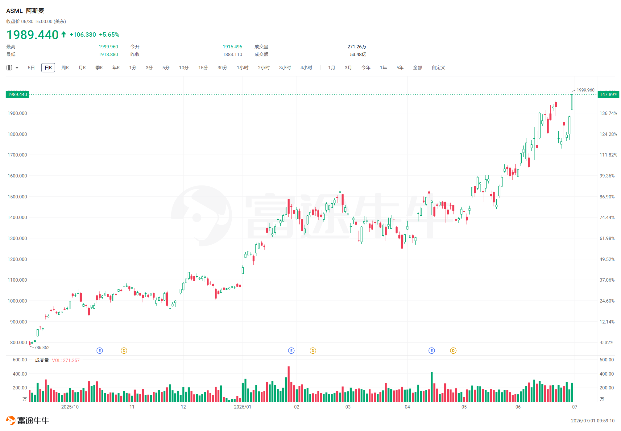
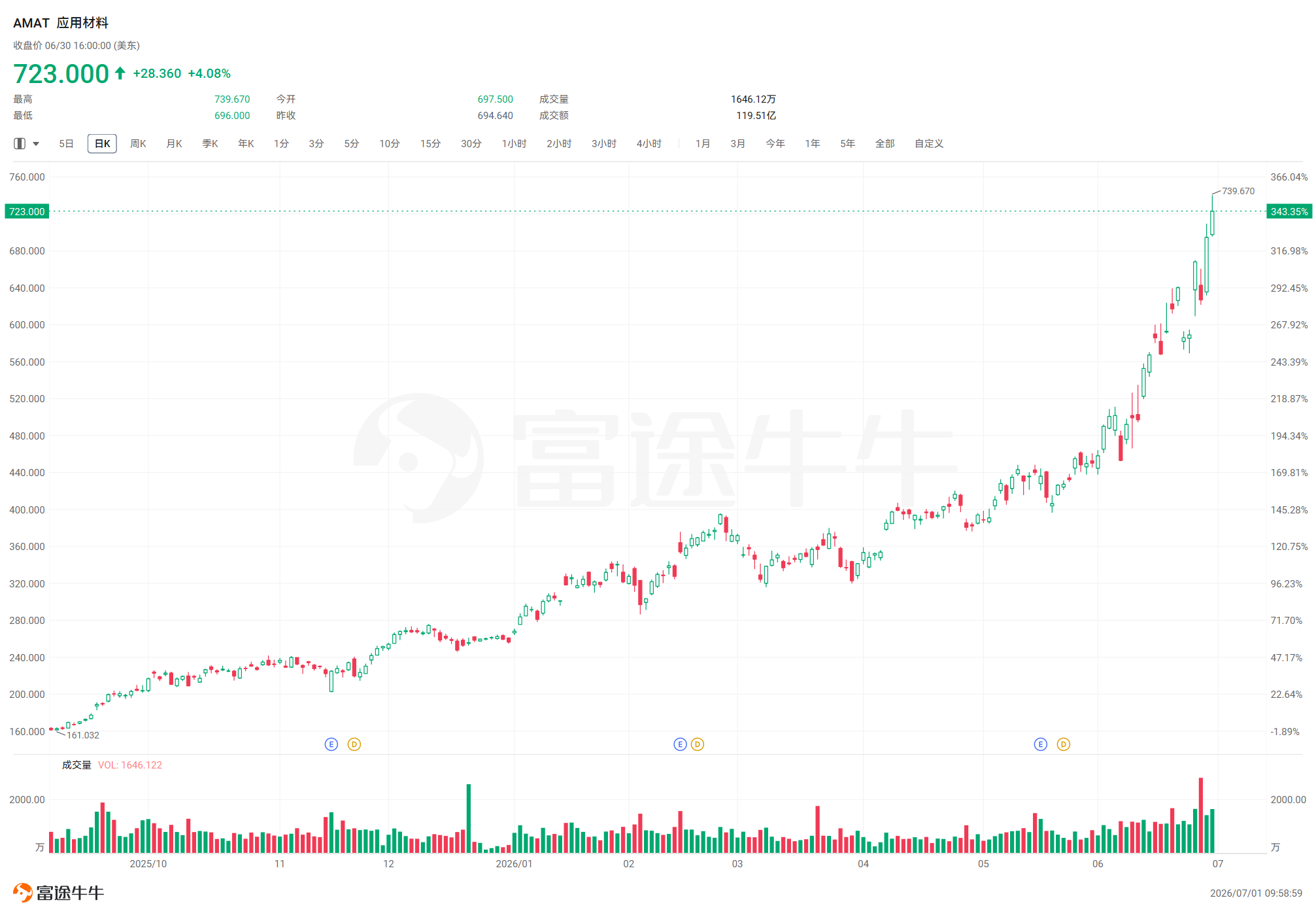
This rally extends the semiconductor sector’s strong performance this year. The Philadelphia Semiconductor Index nearly doubled in the first half of the year, surging over 86% in the second quarter—the strongest quarterly gain on record. However, volatility remains pronounced: the index dropped 7.9% in a single week last week, its worst weekly performance since early April, before rebounding as investors returned to artificial intelligence infrastructure-related equities.
Susquehanna analyst Mehdi Hosseini maintains a bullish outlook on semiconductors, citing sustained strength in industry demand. Other institutions forecast that global annual spending on wafer fabrication equipment will reach USD 250 billion by 2028.
New Memory Chip Cluster in Southwestern Korea
At the core of this investment plan is the creation of a new memory chip cluster in southwestern Korea, with total planned investment of approximately KRW 800 trillion (about USD 518 billion), aiming to double DRAM capacity within five years. Samsung and SK Hynix will each construct two fabs, while the government will provide supporting infrastructure including land, power, and water supply.
Separately on June 29, Samsung also announced a longer-term domestic investment plan: between 2026 and 2040, it will invest KRW 2,450 trillion domestically, of which approximately KRW 2,100 trillion—76%—will be allocated to semiconductors.
Analysts at Goldman Sachs, led by Giuni Lee, provided a detailed breakdown:
KRW 1,650 trillion will be allocated to existing and under-construction wafer fabs, including accelerating the completion timeline of the Yongin Fab 6 from 2047 to 2040;
KRW 400 trillion allocated to two new wafer fabs in Gwangju, forming the core of the Southwest Cluster;
KRW 56 trillion earmarked for a new HBM wafer fab in Chungcheong Province.
Goldman Sachs estimates that if Samsung’s domestic capital expenditure and R&D combined account for approximately 80% of its consolidated total, and assuming an average annual growth rate of around 6%, cumulative domestic spending from 2026 to 2040 would amount to roughly KRW 2,500 trillion—broadly consistent with official announcements. Based on this, Goldman Sachs concludes, "This implied spending growth rate is not aggressive."
Capacity doubles, but actual growth is far more moderate than the headline figure suggests.
Korean memory chipmakers have reaffirmed their goal of nearly doubling DRAM wafer capacity by 2030, but analysts at Bank of America Securities, led by Simon Woo, tempered expectations in a research report published on June 29–30.
While doubling sounds aggressive, it corresponds to a compound annual growth rate (CAGR) of only about 15%. More importantly, when factoring in the closure of older fabs and the longer manufacturing cycles required for next-generation memory chips, the actual annual growth rate of operational wafer capacity will be below 10%, resulting in a net wafer capacity CAGR in the single-digit percentage range by 2030.
Bank of America Securities also noted that the new Southwest Cluster is located far from the Seoul metropolitan area, requiring significantly greater infrastructure investment and presenting construction challenges markedly higher than those at existing sites such as Pyeongtaek and Yongin. The firm likened this strategy to Taiwan Semiconductor’s decentralized layout in Tainan, arguing that capacity expansion away from core regions demands a substantially longer lead time for preparatory work.
Taking into account infrastructure development (at least five years) plus wafer fab shell construction and ramp-up (an additional three to four years), Bank of America Securities judges that meaningful volume production from the new cluster will not occur until at least eight to ten years from now.
For the semiconductor equipment sector, the next critical milestone is the July earnings season. ASML is scheduled to release its results on July 15, followed closely by Taiwan Semiconductor on July 16. Investors will closely monitor both companies’ latest guidance on capital expenditures for new fabs, which will directly shape expectations for equipment demand.
Editor/KOKO