
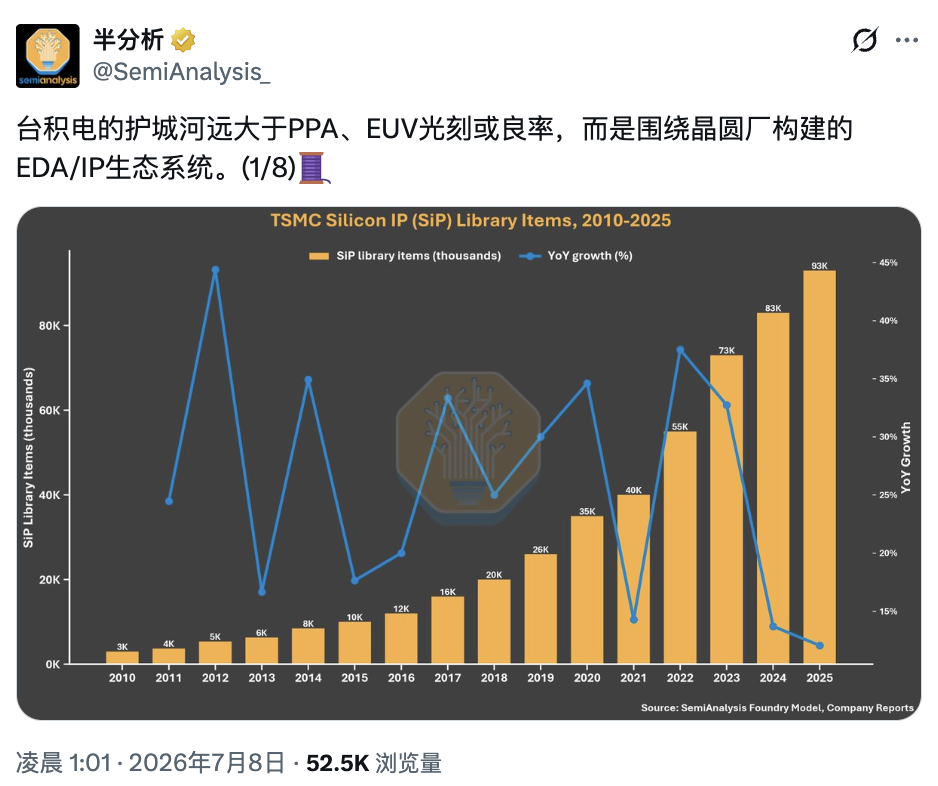
SemiAnalysis noted that Taiwan Semiconductor has deeply integrated EDA design tools, silicon IP, and manufacturing processes. Its certified silicon IP library has grown from approximately 3,000 items in 2010 to 93,000 by 2025, creating a virtuous feedback loop. At advanced nodes, a single tape-out failure can cost over $100 million, making risk reduction in design more critical than merely pursuing improvements in performance, power, and area (PPA). This tight integration significantly raises the total cost for customers to switch foundry suppliers, rendering them 'unwilling and afraid to migrate.'
On July 8, prominent semiconductor research firm SemiAnalysis posted eight consecutive tweets stating, $Taiwan Semiconductor (TSM.US)$ The truly difficult-to-replicate competitive moat lies not in advanced process nodes, EUV lithography tools, or yield advantages, but in the EDA and IP ecosystem built around the foundry.
The firm argues that the market has long attributed Taiwan Semiconductor’s strength to PPA (performance, power, area) optimization. However, what ultimately determines whether customers stay or leave is whether their entire design risk framework can seamlessly migrate alongside the foundry. Taiwan Semiconductor’s ecosystem continuously reduces customers’ tape-out risks while substantially increasing the total cost of switching suppliers.
 Therefore, Samsung Foundry and Intel Foundry face not only process technology competition but also an ecosystem battle. Customers will not easily switch foundries simply because a competitor claims superior PPA; their willingness to migrate hinges on the full portability of their design tools and IP assets.
From 3,000 to 93,000: Certified IP Library Builds an Ecosystem Moat
SemiAnalysis believes the most tangible manifestation of Taiwan Semiconductor’s moat is its continually expanding certified IP ecosystem.
Data shows that Taiwan Semiconductor’s Open Innovation Platform (OIP) has integrated EDA and IP vendors—including Synopsys, Cadence, Arm, Rambus, and Alphawave—into a unified pre-validated tape-out network. Its certified silicon IP library has grown from approximately 3,000 items in 2010 to 93,000 by 2025—an increase of over 31-fold in 15 years—covering critical building blocks such as SerDes, HBM, PCIe, UCIe, memory interfaces, and chiplet interconnects.
These pre-certified IPs significantly reduce design risk for customers taping out at Taiwan Semiconductor while markedly increasing the cost of migrating to other foundries.
SemiAnalysis points out that this creates a self-reinforcing positive feedback loop: the foundry enhances customer stickiness through its EDA/IP ecosystem, while EDA vendors attract more design projects by securing process certifications, further solidifying their own market positions. What Samsung and Intel truly need to replicate is not a single advanced node, but this ecosystem cycle built through long-term accumulation.
An $18 billion market, with the Big Three forming the industry foundation
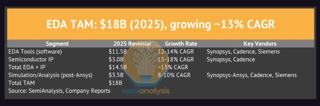
Behind this ecosystem lies a highly concentrated EDA industry. According to SemiAnalysis, the global EDA and IP market was valued at approximately $18 billion in 2025 and is projected to expand to between $28 billion and $30 billion by 2030.
Synopsys, Cadence, and Siemens EDA collectively account for over 85% of the market share. Based on fiscal year 2025 figures, Synopsys (including Ansys) reported revenue of approximately $8 billion, Cadence around $5.3 billion, and Siemens EDA between $2.2 billion and $2.5 billion.
Over the past decade, the EDA industry has maintained steady growth, with a compound annual growth rate (CAGR) of approximately 13%, significantly outpacing the growth rate of semiconductor R&D spending during the same period. Since 2018, this gap has widened further, primarily driven by AI chip development, increasing complexity in advanced-node verification, and rapidly growing demand for hardware emulation.
Citing prior remarks by Synopsys CEO Sassine Ghazi, SemiAnalysis noted that the design complexity introduced by AI is pushing the semiconductor industry’s R&D spending as a percentage of sales from approximately 6% toward 9%, benefiting EDA vendors through both expanded R&D budgets and increased verification workflows, AI-assisted design tools, and enhanced pricing power at advanced nodes.
What truly locks in customers is design risk—not PPA
In SemiAnalysis’s view, the core of competition in advanced process technologies is not performance metrics, but design risk.
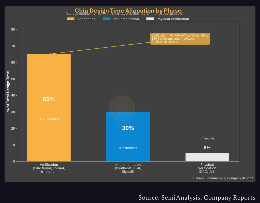
The report notes that at advanced nodes, a single re-spin typically costs between $50 million and $100 million and can delay product time-to-market by six to twelve months. Therefore, for large chip design companies, reducing the risk of design failure is often more critical than achieving marginal improvements in PPA (power, performance, and area).
From RTL synthesis and place-and-route to signoff analysis and physical verification, the modern chip design flow has evolved into a tightly integrated toolchain. Any change to a core EDA tool can necessitate re-execution of all downstream verification steps. The report states: "The entire flow itself is the lock-in."
Similarly, Taiwan Semiconductor-certified IP blocks—such as SerDes, HBM, and PCIe—are deeply integrated with process design kits (PDKs). If a customer wishes to migrate a flagship ASIC to another foundry, they must not only rebuild their EDA toolchain but also revalidate a significant volume of IP.
Therefore, SemiAnalysis believes that Taiwan Semiconductor's true competitive moat lies not in a single process advantage, but in an integrated 'design risk mitigation ecosystem' comprising EDA certifications, IP validation, and PDKs.
Competitors are racing to catch up on more than just advanced nodes.
This also explains why the challenges faced by Samsung Foundry and Intel Foundry in closing the gap are far greater than commonly perceived.
SemiAnalysis notes that even if competitors narrow the gap in process metrics in the future, they will still need to rebuild the decades-old collaborative ecosystem with EDA vendors and IP suppliers—a task far more time-consuming than improving transistor performance.
The report also cites Intel Foundry as an example, pointing out that its recent shift in focus for external customers from the 18A node to 18A-P and subsequent nodes has delayed the commercialization of certain IPs originally developed around 18A, thereby negatively impacting related EDA vendors’ IP revenue. This illustrates how adjustments to a foundry’s technology roadmap not only affect manufacturing itself but also ripple through the EDA and IP ecosystem across the entire supply chain, further reinforcing customer reliance on mature design ecosystems.
SemiAnalysis argues that in the era of advanced process nodes, the competitive landscape of foundry services is no longer determined solely by PPA, EUV adoption, or yield—but by which player can establish a comprehensive design ecosystem that makes customers 'unwilling and afraid to switch.' This constitutes Taiwan Semiconductor’s most difficult-to-replicate competitive advantage.
Editor/lambor