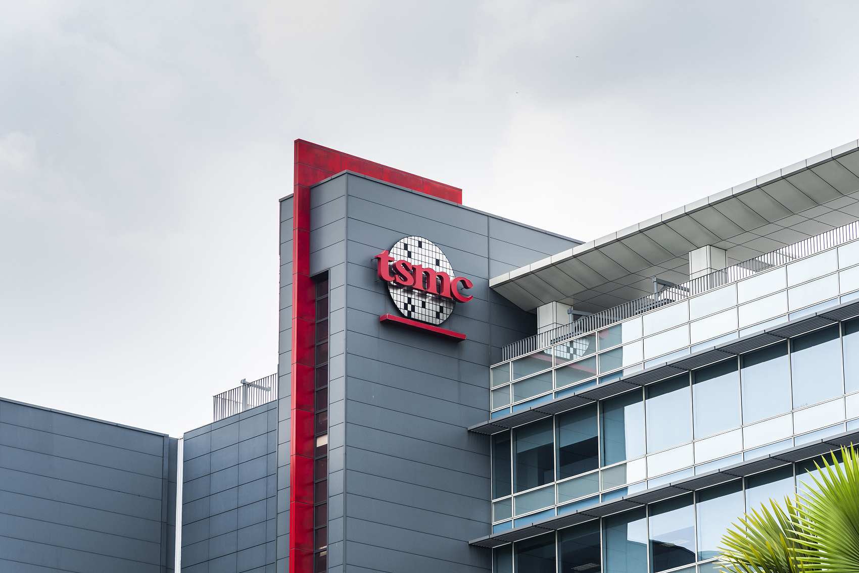
Demand for AI chips continues to surge, and Taiwan Semiconductor is reshaping the global advanced packaging landscape at an unprecedented pace. With the groundbreaking of its Chiayi Phase II facility and the establishment of two fabs in Arizona, U.S., its CoWoS capacity is booked through 2027, with a compound annual growth rate exceeding 80%. Revenue from advanced packaging is projected to surpass 15% of total revenue by 2027, officially becoming Taiwan Semiconductor’s second core growth engine following advanced process technology.
Taiwan Semiconductor is accelerating advanced packaging from a supplementary step in wafer fabrication to an independent strategic growth engine through an unprecedented pace of capacity expansion. The Phase II site at the Chiayi Science Park has officially commenced, complemented by its dual-fab layout in Arizona, USA, enabling Taiwan Semiconductor to simultaneously expand its advanced packaging footprint across Taiwan and North America.
Phase I of the Chiayi Science Park began mass production in June this year, and the third packaging facility within Phase II broke ground in the same month—two milestones achieved within 30 days. Around the same time, Taiwan Semiconductor signed a 10-year long-term agreement with packaging and testing giant Amkor to build two packaging plants in Arizona. Brokerage firms estimate that advanced packaging will account for over 10% of Taiwan Semiconductor’s revenue this year for the first time, rising further to more than 15% by 2027, establishing it as the company’s second primary growth pillar after advanced process technology.
 This round of capacity expansion is directly driven by sustained stronger-than-expected demand for AI chips. Taiwan Semiconductor’s CoWoS capacity will remain fully utilized from 2024 through 2026, with order visibility extending into 2027. The company plans for CoWoS capacity to grow at a compound annual growth rate (CAGR) exceeding 80% between 2022 and 2027, and SoIC capacity to grow at a CAGR above 90%—a near-doubling pace annually, making large-scale fab construction an inevitable choice.
Chiayi Cluster: The World’s Largest Advanced Packaging Hub Accelerates Toward Completion
Phase II of the Chiayi Science Park spans approximately 90 hectares and is planned to attract emerging industries such as AI, heterogeneous integration, and quantum technology, with full development targeted for completion by 2031. Taiwan Semiconductor’s third advanced packaging facility within Chiayi Science Park Phase II officially commenced construction in June this year. The first and second packaging plants (AP7) in Phase I are currently in the equipment installation phase and are expected to achieve stable mass production by 2027.
Taiwan Semiconductor stated that it plans to add a third and fourth plant, along with room for further expansion. Industry sources noted that with Phase II land now secured, the company could potentially construct three or more additional facilities. The combined Phase I and Phase II developments at Chiayi Science Park are projected to generate annual revenue of NT$313.2 billion and create 9,200 jobs.
In terms of technology roadmap, equipment vendors assess that the initial focus of AP7 in Chiayi Phase I will be on Apple-specific Wafer-Level Multi-Chip Module (WMCM) packaging, gradually transitioning to high-end processes such as SoIC and CoWoS in the future. Geographically, the Chiayi park complements the 2-nanometer volume production base at Fab 22 in Kaohsiung and the A14 advanced node at Fab 25 in Central Taiwan Science Park (CTSP). Starting with the 2-nanometer generation and beyond, the value of a single chip will be jointly determined by 'advanced process technology plus advanced packaging,' positioning the Chiayi cluster as a pivotal node linking advanced supply chains across southern and central Taiwan.
Capacity Expansion: Supply-Demand Pressure Behind 80% Compound Annual Growth
Taiwan Semiconductor has already deployed advanced packaging facilities across six locations island-wide—in Taoyuan, Hsinchu, Miaoli, Taichung, Tainan, and Chiayi—and market reports suggest the company is considering adding a new plant at the Erhlin campus of Central Taiwan Science Park.
Demand-side pressure is clearly evident. Leading customers—including NVIDIA, AMD, Google, and AWS—are continuously advancing designs for large-scale AI accelerators, keeping Taiwan Semiconductor’s advanced packaging capacity fully loaded. As technologies like CoWoS and SoIC rapidly enter volume production, packaging is no longer merely a back-end process but has become a critical determinant of AI chip performance, power efficiency, and system-level integration capabilities.
Of its projected $56 billion in capital expenditures for 2026, Taiwan Semiconductor will allocate approximately 10% to 20%—equivalent to $5.6 billion to $11.2 billion—to projects related to advanced packaging and testing, mask production, and associated activities. This marks a strategic shift, elevating advanced packaging from a supporting component of capital spending to an independent strategic investment focus.
Dual Arizona Facilities: A Decade-Long Agreement Anchors Domestic U.S. Capacity
While aggressively expanding capacity in Taiwan, Taiwan Semiconductor is partnering with Amkor to establish a North American foothold for its advanced packaging capabilities. Under this 10-year cooperation agreement, Taiwan Semiconductor will utilize Amkor’s advanced packaging and testing services and plans to construct two advanced packaging facilities in Arizona, with the first already having applied for construction permits.
The strategic value of this move lies in localizing a closed-loop supply chain. With Taiwan Semiconductor’s 4-nanometer and 3-nanometer wafer fabrication plants already under construction in Arizona, the addition of packaging capacity will enable U.S. customers to complete the entire process—from wafer manufacturing to packaging and testing—within a single region, significantly reducing cross-border supply chain risks.