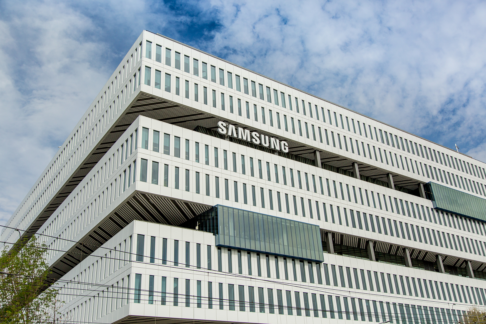
A turning point has arrived! Driven by dual demand from HBM and AI, Samsung Foundry’s capacity utilization rate in the second half of the year is expected to approach 100%, with profitability potentially returning as early as Q3. However, securing mass production orders from major clients like Qualcomm will ultimately hinge on surpassing the critical 70% yield threshold for its 2-nanometer process node.
Samsung Electronics' foundry business is reaching a critical inflection point. Driven by demand for HBM base chips and orders from major U.S. tech companies, the division’s capacity utilization rate is expected to reach 100% in the second half of this year, potentially marking a turning point in its chronic loss-making structure that has persisted for over a year.
According to South Korea’s Chosun Ilbo, Samsung Foundry’s current capacity utilization is estimated to be in the 70%–80% range. Combined with existing order backlogs and ongoing contract execution, achieving full utilization this year is "virtually certain." During its second-quarter earnings call, Samsung Electronics stated that utilization rates across all process nodes have improved compared to the same period last year, with advanced nodes below 8 nanometers already at "peak levels." The company also projected that orders for its 2-nanometer projects this year will more than double compared to last year. While it refrained from specifying an exact timeline for returning to profitability, it noted that such a turnaround is "achievable in the near future."
 Market analysts expect Samsung’s non-memory businesses—including foundry and System LSI—to return to profitability as early as the third quarter and no later than the fourth quarter. If normalized capacity utilization coincides with rising wafer prices, the pace of earnings improvement could exceed market expectations.
Dual drivers of HBM and AI demand accelerate utilization gains
The rebound in capacity utilization is primarily driven by two key factors: first, the sixth-generation high-bandwidth memory (HBM4), manufactured on a 4-nanometer process, directly channels the memory sector’s upcycle into the foundry business; second, cloud service providers (CSPs) and customers in AI and high-performance computing (HPC) are increasingly demanding 2-nanometer process technology, with project discussions already underway with major clients such as Broadcom.
This context is particularly noteworthy: since 2024, Samsung Foundry’s capacity utilization has remained persistently below 50%, leaving high fixed costs inadequately covered and resulting in continuous losses. Given the massive capital investment required for semiconductor foundry operations, idle production lines lead to rapidly accumulating losses over time; conversely, once utilization returns to normal levels, incremental revenue translates directly into profit.
Diversifying customer base, but 2-nanometer yield remains a critical hurdle
In terms of customer composition, Samsung Foundry is accelerating efforts to reduce overreliance on a single major client. Tech giants including Qualcomm, AMD, and Google have already entered negotiations, and Tesla is reportedly planning to produce its next-generation chips using the 2-nanometer process. As a result, the mid- to long-term order pipeline is significantly strengthening.
However, industry observers widely agree that converting these potential clients into large-scale mass production contracts hinges critically on whether the 2-nanometer process yield can stabilize above 70%. Current estimates place the yield around the 60% mark, still short of the threshold required for volume production. An industry insider remarked, "Normalization of utilization is a leading indicator that the foundry business has crossed the breakeven point, but confirming a substantive improvement in operational health will require stable 2-nanometer yields and actual mass production commitments from major clients."
Rising share of advanced nodes accompanied by concurrent capacity expansion
Business portfolio restructuring is also accelerating in parallel. Revenue from advanced process nodes is expected to exceed 50% this year, while revenue related to AI and HPC is projected to surge from around 10% at the end of last year to over 30%. In the second half of the year, mobile products based on the second-generation 2-nanometer (SF2P) process will commence mass production.
On the capacity front, Fab 1 in Taylor, Texas, USA, is progressing as scheduled toward production readiness this year, while Fab 2 in Taylor is slated to break ground within the year, targeting mass production by 2030. As customer inquiries regarding the 1.4-nanometer node increase, plans for additional wafer fabs have also been added to the research agenda.
Analysts at brokerage firms noted that if the positive impact of wafer price increases aligns with the normalization of utilization rates, Samsung Foundry’s profit recovery could occur faster than previously anticipated by the market. However, cautious voices remain: while achieving 100% capacity utilization is undoubtedly important, the true tipping point for flagship customers such as Qualcomm and AMD to initiate large-scale foundry orders hinges on whether 2-nanometer yield can surpass 70%. In other words, normalized utilization marks the starting point for ending losses, but a deeper transformation of the business ultimately depends on continuous breakthroughs in advanced process technologies and tangible mass-production commitments from major clients.